
MacroFab Blog

As seasoned PCBA design engineers, you know how difficult it is to achieve perfection. But to continually enhance system performance, it’s crucial to thoroughly analyze failure modes, identify their root causes, and strategize their elimination.
End-user concerns are primarily centered around service failures, but minimizing them requires examining the design-build-test cycle in detail. It is important to create and rectify failures during this phase so that weaknesses can be addressed before production begins. Here are some tips to avoid common failures, and how MacroFab can help along the way.
Proactively Tackling Electrical Issues
When designing PCBAs, it’s important to recognize potential manufacturing issues. For multi-layer boards, you need to ensure precise alignment between layers to avoid via errors that can cause short circuits or open circuits. Component placement demands accuracy down to fractions of a millimeter, as misalignment and limited solder space can lead to solder bridges or open circuits.
General electromagnetic issues in PCB design often stem from flaws rather than component failures. These issues manifest in various ways, including inadequate ground plane area, sharp corners on PCB traces, lack of shielding cables, and electromagnetic compatibility faults. Addressing these concerns is essential for optimizing circuit board functionality.
To tackle electromagnetic issues, make sure you provide a sufficient ground plane area to enhance conduction and reduce interference. Avoid sharp angles that introduce impedance mismatches and signal reflections. Incorporate shielding cables or metallic protective sheathing to minimize electromagnetic interference. Additionally, pay attention to alignment during the manufacturing of multi-layer boards to prevent circuit disruptions.
Careful component placement is crucial, requiring meticulous planning with proper clearances and adherence to design guidelines to prevent solder bridges and open circuits. The top componentrelated design issues causing failures include
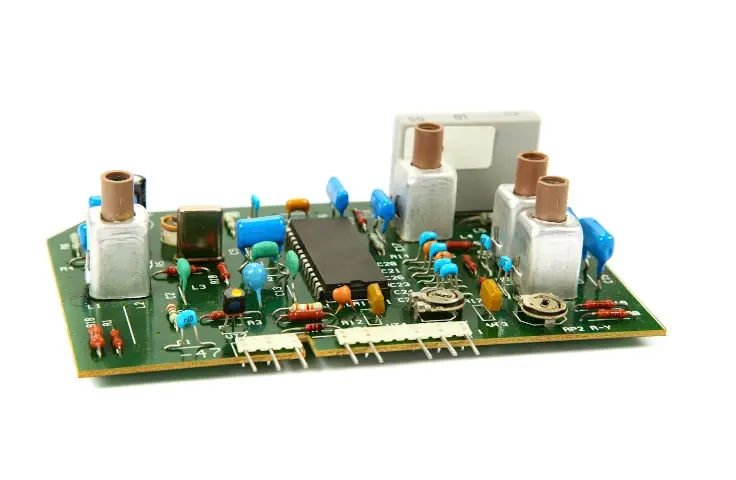
- Tombstoning – Proper component placement is key. A symmetrical design provides equal solder paste and surface tension during reflow, minimizing the chance of tombstoning.
- Solder bridges – Follow DFM guidelines and leave sufficient clearance to avoid solder bridges.
- Misaligned layers – use fiducials or alignment markers as reference points, and plan stackups carefully.
By addressing these considerations in your PCBA design, you can optimize circuit board performance, minimize electromagnetic issues, and contribute to the development of reliable electronic systems.
MacroFab employs Automated Optical Inspection (AOI) to enable early detection of defects like component misalignment, soldering issues, missing components, and bridging. By capturing high resolution images, the AOI system can swiftly identify defects or issues, allowing for immediate corrective action, fostering real-time feedback, and enhancing overall efficiency while minimizing waste.
Want to learn more? Read PCBA Cost and Complexity Design Factors You Should Know now.
Shock and Vibration Management
In the real world, circuit boards face various challenges such as vibration, flexion, strain, torsion, and other shock events. These events can range from sudden impacts after a drop to regular vibrations experienced by mounted PCBAs in vehicles.
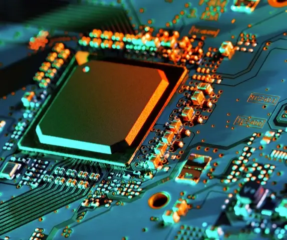
To determine potential PCBA design vulnerabilities to shock and vibration damage, you can utilize physical tests and simulation modeling. By analyzing these results, you can optimize your design to mitigate risks. Consider relocating high-risk components away from strain points, incorporating board stiffeners to reduce torsion, or isolating the board from vibration using shock-absorbing materials like rubber standoffs. Stiffeners can also provide some heat dissipation, so consider that when designing your boards.
MacroFab’s network is able to support you if you require validation of your designs against vibration environments. Verifying the robustness of your design allows you to make necessary improvements to ensure its resilience. By implementing these strategies and conducting thorough validation, you can enhance the durability and reliability of your PCBA, safeguarding it against the effects of shock and vibration.
Want to know more about designing for shock and vibration? Read Ruggedized Electronics Design Basics: How to Increase Your PCBA Lifespan now.
Addressing Mechanical Issues
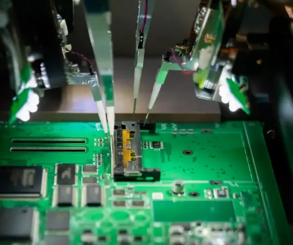
The PCBA you’re designing is just a portion of your final product, destined to snugly fit within a mechanical enclosure. This integration presents its own unique set of challenges that you need to tackle right from the beginning of your product’s lifecycle. It’s crucial to craft your PCBA with the utmost precision to align with the given mechanical dimensions without compromising on the necessary components or their functionality. Try employing 3D modeling software to mitigate any potential fit problems at the early stage of the design process. Such software helps to flag potential layout complications, allowing you to foresee and address issues like components that may be too tall or wide for the enclosure. You want to avoid the unwelcome surprise of a component that won’t fit your enclosure.
Checkpoint
Enclosures can become heat traps, so thermal management is crucial.
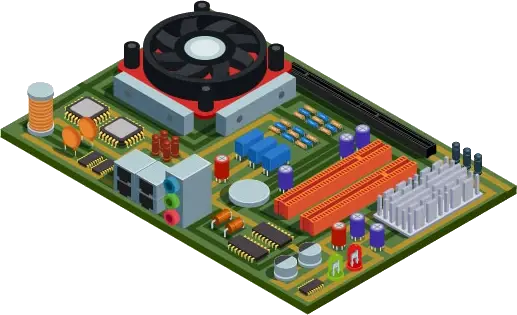
Enclosures can become heat traps, making thermal management crucial. Integrate cooling elements like heat sinks or fans to keep your PCBA at a safe temperature. Ignoring these factors could cause damage and shorten your design’s lifespan.
In addition, design with accessibility in mind for easy maintenance and repair. Strategically place the components prone to needing repair near the mechanical enclosure’s access points.
Leveraging the expertise of a company like MacroFab, specializing in PCB assembly and after-build mechanical box builds, can be beneficial. MacroFab’s team is proficient in detecting and avoiding potential mechanical issues before they manifest, saving you both time and money.
Addressing Premature Field Failures
When premature field failures occur, it’s crucial to have a partner that prioritizes such events and stands by you. At MacroFab, we place great importance on these rare incidents. Our manufacturing processes come with a one-year quality guarantee against manufacturing defects to give you peace of mind.
In the unlikely event of a manufacturing anomaly during the first twelve months, don’t hesitate to contact us. We’ll guide you through the RMA process, making sure it’s sorted out fast. We dive deep into the product’s examination to spot the source of the issue, providing you with regular updates throughout the process. Trust us to tackle any challenge head-on, keeping you informed, and addressing the issue as promptly as possible.
Emphasizing Prevention: Designing for PCBA Success

As PCBA design engineers, understanding and anticipating potential failure modes is a fundamental aspect of your role. By scrutinizing every phase of the design-build-test cycle, and considering both electrical and mechanical stressors, you can construct robust, reliable systems that minimize field failures and maximize customer satisfaction.
By relying on cutting-edge technology such as Automated Optical Inspection and end-of-line testing, MacroFab is here to support you in producing high-quality PCBAs ready for a long and efficient service life.
Related Topics
Mapping Out a PCBA Supply Chain Strategy in Five Moves
Companies should create unique vendor relationships with numerous international suppliers due to the necessity of having to source components globally.
Struggling with Inflexible PCBA Manufacturing? MacroFab's Got Your Back.
Many electronics designers struggle with systems that demand complete data and specific formats upfront. Wouldn't it be great if there was a better way?
Fab Insights: HASL vs ENIG
Choosing the right surface finish for a PCBA can be tricky. HASL and ENIG differ in their methods of coating printed circuit boards.
Ask MacroFab About Mechanical Enclosures for Your Assembly
MacroFab's Box Build AssemblyAbout MacroFab
MacroFab offers comprehensive manufacturing solutions, from your smallest prototyping orders to your largest production needs. Our factory network locations are strategically located across North America, ensuring that we have the flexibility to provide capacity when and where you need it most.
Experience the future of EMS manufacturing with our state-of-the-art technology platform and cutting-edge digital supply chain solutions. At MacroFab, we ensure that your electronics are produced faster, more efficiently, and with fewer logistic problems than ever before.
Take advantage of AI-enabled sourcing opportunities and employ expert teams who are connected through a user-friendly technology platform. Discover how streamlined electronics manufacturing can benefit your business by contacting us today.