PCB Fabrication
PCB and Product Assembly
Engineering Services
Testing and Validation
Component Sourcing
PCB Specifications
Capabilities
Layer Count and Stackups
Surface Finish
Materials
Copper Weight
Soldermask & Silkscreen Colors
Fabrication Processes
Via Fill Options
Board Area
Board Thickness
PCB Assembly
Capabilities
Solder Types
Flux Types
Assembly Supported
Mechanical Component Limits
Depanelization
Machines and Processes
Box Build and Testing
Capabilities
Conformal Coating
Component Programming
Full Product Assembly
Testing and Validation
Design Rules (DRC)
Capabilities
Design Minimums
Tolerances
Quality and Certifications
Capabilities
MacroFab Manufacturing Guarantee
Inspection
IPC-A-610H
MacroFab Facility Certifications
Partner Facility Certifications
IPC-A-610
Learn More About PCBA Capabilities
Choose the Optimal Electronics Manufacturer for New Product Prototyping
As new technologies, capabilities, and manufacturing equipment come into play, the prototyping phase validates the functionality of a new product.
Sourcing, Fabrication, Assembly & Testing Capabilities
MacroFab capabilities include fine-pitch BGA, HDI, and QFN assembly. Download this document for an overview of our fabrication and assembly specifications.
Six PCBA Design Trends to Watch in 2023
Engineers must continually seek out new options and keep up with market changes. Take note of these six trends within the electronics industry.
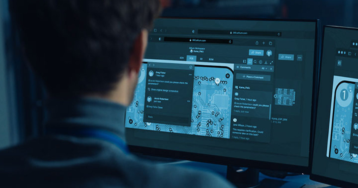
Altimade Fuses Design with Manufacturing
Taking a new design from concept to manufacturing can be difficult, and transferring files to the manufacturer can take unprecedented blocks of time.