Choosing the right surface finish for a Printed Circuit Board Assembly (PCBA) can be tricky. A surface finish is more than just a protective layer—it’s essential for the board’s performance and longevity. It shields the copper circuits from oxidation, aids in soldering components, and can affect the electrical performance of the assembled PCB.
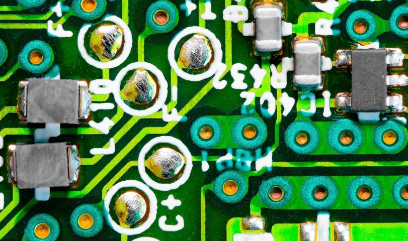
Hot Air Solder Leveling (HASL) has been one of the most common surface finishes for years. This cost-effective and highly solderable surface finish became the industry’s backbone. However, HASL had its limitations, especially regarding planarity and compatibility with certain high-frequency applications. This led the industry to seek alternatives that could overcome these issues.
Among the many alternatives that surfaced, Electroless Nickel Immersion Gold (ENIG) proved prominent, providing excellent planarity performance. However, the choice between HASL and ENIG is not always black and white; it presents a dilemma due to each finish’s unique advantages and disadvantages.
How do HASL and ENIG Differ?
HASL and ENIG differ in their methods of coating printed circuit boards (PCBs). HASL immerses the PCB in molten solder and uses hot air solder to smooth the surface, which can sometimes result in an uneven coating. ENIG, however, applies an electroless nickel layer, then an immersion gold layer to the PCB, offering better surface flatness and oxidation resistance, especially for intricate components. While ENIG may be costlier, its advantages often make it worth the extra investment.
This article explores the pros and cons of HASL and ENIG surface finishes, offering you valuable insights to aid in selecting the best surface finish for your PCBAs.
HASL: Overview, Benefits, and Limitations
Hot Air Solder Leveling is a traditional method used to protect the copper circuitry on a PCB from oxidation. In the HASL process, the PCB is dipped into a bath of molten solder. The board is then leveled with hot air knives, which remove excess solder and create a surface suitable for component soldering.
HASL has primarily two types based on the composition of the molten solder used in the process:
- Lead-based HASL: This is the traditional variant of HASL that uses a tin/lead (Sn/Pb) alloy. The use of lead, though effective, has raised environmental and health concerns. As regulations around using lead have tightened, industries have been motivated to seek alternatives.
- Lead-free HASL: Also known as LF-HASL, this variant has emerged as a response to the environmental concerns of leadbased HASL. The most commonly used alloy in lead-free HASL is tin/copper (Sn/Cu), although there are other variants like tin/copper/silver (Sn/Cu/Ag) and tin/copper/nickel (Sn/Cu/Ni). Note: this is the only kind of HASL finish MacroFab offers.
| Property | Tin-Lead HASL | Lead-Free HASL |
|---|---|---|
| Composition | Tin, Lead | Typically Tin-Copper, Tin-Silver-Copper, or Tin-Nickel |
| Environmental Impact | High (Contains Lead) | Lower (Lead-Free) |
| Performance | Proven reliability, Excellent Solderability | Slightly varied performance based on the exact alloy used |
| Regulatory Compliance | Not compliant with RoHS | Compliant with RoHS and other lead-free requirements |
| Cost | Generally less expensive | More expensive |
Benefits of the HASL Finish
- Solderability: HASL ensures excellent solderability. This makes it a good choice for both manual soldering and wave soldering.
- Cost-effectiveness: HASL is generally less expensive than other surface finishes, making it an attractive option for budget-conscious projects.
- Durability: It is a durable finish with a good shelf life, suitable for a range of general applications.
Limitations of HASL
- Planarity Issues: HASL might present a lack of uniformity and flatness (planarity) on the surface due to the leveling process. This can cause problems for components with fine pitch or high-density components.
- Lead/Lead-Free Options: Traditional HASL uses lead, raising environmental concerns. While lead-free HASL options exist, they can be more expensive and present a different set of challenges, like higher melting points that can affect the thermal management of the PCB.
- Compatibility: HASL is not the best option for specific applications like high-frequency RF applications due to possible signal integrity issues.
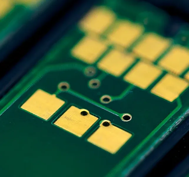
ENIG: Overview, Benefits, and Limitations
An ENIG finish is a double-layer metallic coating. The first layer is a nickel-phosphorus alloy applied via an electroless (autocatalytic) deposition process. The second layer, a thin gold plating coat, is applied using an immersion process.
ENIG plating is markedly softer compared to hard gold plating. It contains grain sizes that are about 60 times larger. It offers hardness in the range of 20 to 100 HK25. For a contact force of up to 35 grams, ENIG plating stands up well. But it doesn’t usually hold up for as many cycles as hard plating.
Gold’s resistance to oxidation and corrosion protects the underlying nickel, making it ideal for long storage periods, even when the PCB is not immediately used post-production.
Gold’s properties extend beyond protection. It’s an excellent electricity conductor and decreases the overall contact resistance of the PCB surface, a crucial feature for high-performance or sensitive electronic devices.
Additionally, ENIG is lead-free, making it compliant with RoHS regulations to minimize hazardous substances in electronics. As the trend leans towards environmentally friendly materials, ENIG has gained traction, becoming a goto choice for PCB surface finish.
Benefits of the ENIG Surface Finish
- Flat Surfaces: ENIG provides an exceptionally flat surface, which is excellent for PCBs with fine-pitch components and chip-scale packages (CSPs).
- Highly Reliable: It offers reliable surface planarity for IC substrates and an excellent surface for aluminum wire bonding.
- RoHS Compliant: The ENIG process is lead-free, making it suitable for RoHS-compliant applications.How to Select the Right QFN Package for Your PCBA Project
Limitations of ENIG
Traditional HASL uses lead, raising environmental concerns.
- Costly: ENIG is more expensive than HASL, which may not be suitable for projects with tight budgets.
- Black Pad Syndrome: ENIG sometimes suffers from a problem known as Black Pad Syndrome, an electrochemical migration issue that causes unreliable interconnections.
- Not Ideal for Rework: It may not be as suitable for rework due to the nickel layer’s potential to corrode under intense heat.
Impact on Signal Integrity, Thermal Management, and Reliability
- Signal Integrity: Due to its flat and smooth finish, ENIG is typically favored for high-frequency applications where signal integrity is a top concern. HASL’s irregular surface can introduce impedance variations.
- Thermal Management: HASL’s excellent thermal resistance makes it ideal for applications with multiple reflow processes. However, the thermal performance of ENIG is also sufficient for most common applications.
- Reliability: Both finishes are reliable, but each has its weaknesses. HASL’s uneven surfaces can cause issues with smaller components, while ENIG’s black pad syndrome can lead to unreliable interconnections.
Conclusion
The decision between HASL and ENIG hinges on your project’s specific needs. HASL’s affordability and high thermal resistance are advantageous for budget-constrained projects or those necessitating multiple reflow processes.
Conversely, ENIG’s flat surface, combined with its RoHS compliance, is well-suited for high-frequency applications, fine-pitch components, and eco-friendly products.
MacroFab’s default surface finish is ENIG, primarily because of its co-planar surface. This is key for fine-pitch parts and bottom-terminated components like QFNs and BGAs. Using ENIG can result in a reduction in tombstoning in smaller chip components (think 0402 and 0201 or smaller) by having a smoother surface and a more consistent reflow liquidus stage.
If you need clarification on which surface finish to choose, feel free to reach out to MacroFab, a leading PCBA fabricator. Our experts can guide you, ensuring you select the right surface finish for a high-yield, cost-effective design that meets your performance expectations.
Want to learn more about surface finishes? Read our comparison of ENIG vs ENEPIG.
The MacroFab Platform
Experience a seamless interface that connects sourcing and production to accelerate your iteration process.