The Impact of AI on PCBA Design: What You Need to Know
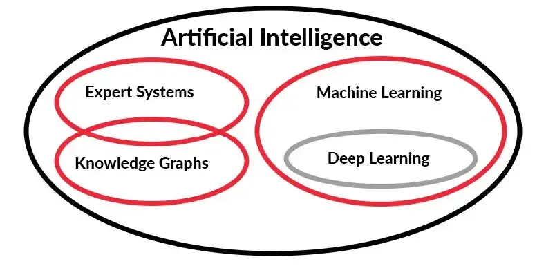
Artificial intelligence (AI) has emerged as a key tool in various fields, including Printed Circuit Board Assembly (PCBA) design, where it enhances efficiency and accuracy. The PCBA industry, which demands high levels of precision and customization, faces complex manufacturing processes, a high labor demand, and significant costs.
Can AI revolutionize PCBA design? This blog dives into 7 ways AI could supercharge everything from component placement to optimizing signal integrity. But it also looks at the challenges of integrating this exciting technology, offering a balanced perspective on the future of AI in PCBA design.
Seven Ways Artificial Intelligence Improves PCB Design
Checkpoint
Executives cited an "increasingly dynamic and competitive environment" as the driving force behind AI adoption.
According to Microsoft’s latest report on AI in Manufacturing, 81 percent of companies surveyed believe AI has become more important. Executives cited an “increasingly dynamic and competitive environment” as the driving force behind AI adoption. Many executives, however, see a continuing knowledge gap as a result of a lack of data from legacy practices.
Once the gap is closed, artificial intelligence holds particular promise for the industry, with its applications poised to address the following:
Routing Optimization
PCBA design and production are dominated by the physical design phase, which includes placement and routing. This can take up over 30 percent of costs and time. The use of automatic placement and routing has been crucial in reducing these figures and lowering production times, costs, and the likelihood of errors.
Recent advancements in Machine Learning (ML) and Deep Learning (DL) have led to the development of AI-assisted design tools that increase automation in the physical design phase. These tools use ML algorithms to quickly and accurately predict routing information early in the design process. They also apply convolutional networks to forecast routing congestion. This allows for early adjustments to the design, improving efficiency.
The key to these improvements is data. With the proper training, AI models learn to recognize relationships between via size, the number of PCB layers, and electrical constraints. Once trained, they can suggest efficient solutions. Options abound, including rule-based systems, supervised learning models, and evolutionary algorithms.
Additionally, ML algorithms help identify potential crosstalk issues before routing, enabling designers to adjust placements and reduce interference ahead of time. ML models are also useful in estimating important design parameters such as wire length, timing, circuit area, and power consumption early on, which aids in making more informed design decisions.
The integration of AI into PCBA‘s physical design phase makes the process faster, more cost-effective, and more reliable by providing early insights into potential design issues.
Despite this, AI tools can’t handle highly complex or novel PCB assembly designs because they don’t have enough training data. Because AI tools usually don’t explain why they pick a certain layout, engineers need to be able to identify and correct errors when they happen.
AI Enhances Signal Integrity in PCBA Designs
Fig. 2 Source
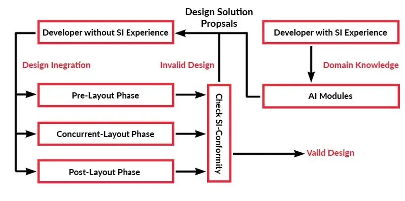
Fig. 2
Signal integrity (SI) is crucial for the functionality of microelectronic components
in PCB assemblies. Achieving optimal SI can be challenging due to the complex nature of interconnect structures. Even experienced PCBA designers often need multiple design cycles to fine-tune parameters, leading to a lengthy and expensive process. When you’re new to SI design, meeting the constraints can be scary.
The use of AI technology could help address these challenges since it can develop predictive models and make design suggestions that make PCBA design more efficient. However, as discussed above, training data quality plays a crucial role in the accuracy of AI predictions.
A recent use-case study highlights the use of three ML techniques—neural network (NN) regression, genetic algorithms (GA), and K-nearest neighbor (KNN)—to analyze PCB net structures. These methods help understand the relationship between electrical parameters and signal quality, enabling the selection of optimal design solutions and direct optimization of interconnect parameters, thus enhancing signal integrity in PCBA designs.
Suggestions made by AI should still undergo human validation, especially for critical designs.
Counterfeit Component Detection
The PCBA supply chain faces significant reliability and security issues. A report from the Defense Industrial Base highlighted that integral components like ICs, resistors, capacitors, and transistors, despite being crucial to PCBAs, are frequently counterfeited.
To combat this, computer vision and machine learning algorithms are being deployed to enhance PCBA inspection methods. These advanced technologies are capable of identifying out-of-spec, defective, reused, and recycled components, thereby increasing the precision of automated inspection processes.
By leveraging smarter inspection tools, manufacturers can more effectively verify the integrity of PCB assemblies. This not only improves the quality of the products but also supports faster validation of PCBAs, crucial for maintaining competitive time-to-market schedules.
While AI can automate much of the inspection process, it cannot replace human expertise entirely. Work with a manufacturer that has a team of experienced technicians that can–and does–review flagged components, especially those not easily identified by artificial intelligence.
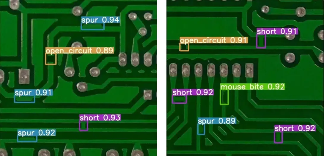
Fig 3. Recognition results of the four defects of spurs, short circuit, open circuit, and mouse bites.
Source
Defect Component Detection
The PCBA industry’s evolution towards miniaturization and increased functionality has heightened the challenge of detecting surface defects such as spurs, mouse bites, short circuits, and open circuits. Traditional Automated Optical Inspection (AOI) systems often misjudge good PCBAs as defective due to minor variations in lighting or soldering, leading to high false positive rates.
To address AOI inaccuracies, some manufacturers rely on manual reinspection, adding labor costs. However, a promising solution is emerging: deep learning algorithms, particularly convolutional neural networks, are being used to improve defect detection. These AI powered systems offer a more accurate and efficient way to identify issues like spurs and mouse bites.
While AI holds immense potential, on-site PCBA assurance remains crucial within trusted environments. PCBA assurance involves testing and inspection to maintain quality and integrity throughout manufacturing and assembly. Traditionally, this relied heavily on manual inspections by experts. While valuable, this method can be slow and prone to errors due to the increasing complexity of PCBAs.
Advancements in AI have led to the development of models trained on high-resolution images of PCBAs, capable of accurately identifying components and detecting a range of defects. This AI-driven approach is setting new standards in PCBA quality control, reducing the reliance on manual inspections and enhancing the overall reliability of PCBAs.
However, human involvement remains important. Collaboratively building the AI’s dataset helps everyone understand why the AI flags certain images. This human-in-the-loop approach aids in weeding out false negatives, identifying missed defects, and reducing bias in the AI system.
AI Assists in Reflowing Complex Assemblies
In PCB assembly, the reflow soldering process follows a specific temperature curve, known as the reflow profile. This profile is pivotal as it ensures the solder melts and flows properly, securing strong and reliable connections between the components and the circuit board without causing damage.
Crafting the perfect reflow profile for complex assemblies is a significant challenge due to the variety of component types, sizes, and thermal properties. An unsuitable profile can result in inadequate or excessive heating, compromising solder integrity and potentially harming heat-sensitive components.
AI is now being used to tackle this issue by determining the ideal heating zones and conveyor speeds in reflow ovens, especially for PCBAs with large components or high thermal mass.
One study showcases AI’s ability to precisely predict the necessary reflow profiles for complex components such as Ball Grid Array (BGA) packages. Another study shows an AI-Driven Smart Recipe Generator to generate effective reflow recipes. These advancements are key to improving the soldering process’s efficiency and ensuring the durability and reliability of the solder joints.
As algorithms are trained, human expertise should continue to check AI outcomes as it gains a better understanding of reflow oven types, materials, and component characteristics.
AI Algorithms as Design Assistants
AI algorithms are now key tools in speeding up electronics design, cutting cycle times by 25 to 50 percent, and raising product quality. ML is useful for performance prediction, where a model predicts how well new designs will perform by learning from past designs. This helps engineers quickly evaluate new ideas without long synthesis steps.
AI can learn from experienced PCBA designers’ knowledge, gathered through interviews, to advise on design decisions. This AI design advisor model can suggest improvements in performance, testability, and production success, making the design process more efficient and less dependent on manual expertise. Additionally, it can be used to predict and optimize heat dissipation, while maintaining predetermined costs.
However, the quality of training data is crucial, and any result should be understood and verified by humans. Moreover, the absence of standardized
classification for PCB components adds complexity. Components may be misidentified due to variations in appearance and functionality across different
manufacturers or design years. The prevalence of certain components over others can bias the AI, and factors like lighting or camera angle can further
complicate component recognition.
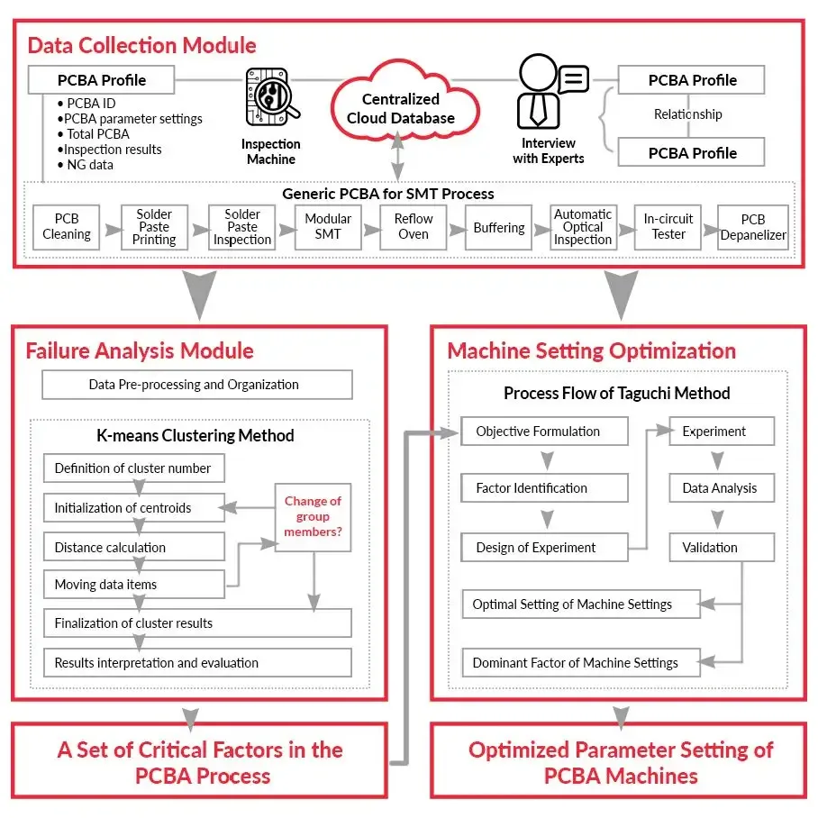
Smart PCBA Manufacturing
PCB assembly and manufacturing face several challenges, including complex production processes, high-quality standards, and fluctuating demand. These complexities can lead to inefficiencies, increased waste, and higher costs. AI is transforming this sector by making manufacturing smarter and more efficient.
Traditional manufacturers are at a disadvantage because they rely on outdated, manual processes. These can’t keep up with the efficient and cost-saving techniques that data and AI offer. Smart manufacturing combines manufacturing with data and AI, dramatically improving supply chain management in several ways:
- Accurate demand forecasting: By analyzing data, manufacturers can predict what and how much to produce, reducing waste
and overstock. - Cost-effective transportation: AI can optimize logistics, finding the most efficient routes and modes of transport to save on
shipping costs. - Automated warehouse operations: Tasks like inventory management and order fulfillment can be automated, saving time and
labor costs.
The result is a streamlined, efficient, and cost-effective manufacturing process. This allows companies using smart manufacturing to adapt to market changes faster and compete more effectively. In short, data and AI offer significant advantages over traditional methods.
Want to see Smart Manufacturing In Action? Schedule a MacroFab Platform Demo Now
Conclusion
AI is revolutionizing PCBA design, offering significant advantages that traditional methods cannot match. From improved routing and signal integrity to counterfeit component detection and automated assembly, AI streamlines the entire process. Additionally, AI-powered PCB manufacturing optimizes production and reduces waste.
However, challenges like ensuring transparency and managing data quality require careful consideration. If AI can solve these hurdles, PCBA design will be a thing of the future. Electronics manufacturing will benefit from its ability to constantly learn and improve.
Related Topics
How to Shorten PCBA Production Lead Times with MacroFab
In the rapidly evolving electronics sector, extended production lead times are no longer tolerable, and minimizing these lead times is crucial for success.
From Garage to Growth: How Startups Scale with MacroFab
Scale your hardware startup smarter with MacroFab—prototype to production, U.S. manufacturing, instant quoting, and expert support every step.
PCBA Order Lead Time Report: Guidance for Lunar New Year 2025
With Lunar New Year coming up, MacroFab wants to ensure they give the best guidance when planning orders to continue meeting delivery guidelines.
Ready to get started?
Get an Instant Quote NowAbout MacroFab
MacroFab offers comprehensive manufacturing solutions, from your smallest prototyping orders to your largest production needs. Our factory network locations are strategically located across North America, ensuring that we have the flexibility to provide capacity when and where you need it most.
Experience the future of EMS manufacturing with our state-of-the-art technology platform and cutting-edge digital supply chain solutions. At MacroFab, we ensure that your electronics are produced faster, more efficiently, and with fewer logistic problems than ever before.
Take advantage of AI-enabled sourcing opportunities and employ expert teams who are connected through a user-friendly technology platform. Discover how streamlined electronics manufacturing can benefit your business by contacting us today.