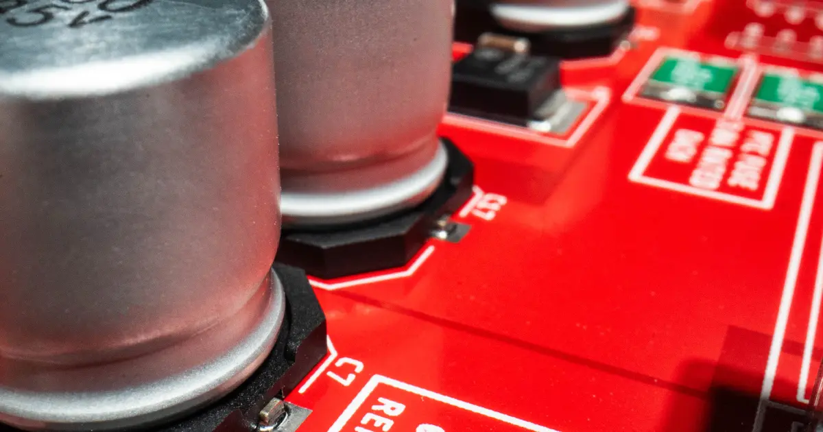
Design rules and layouts are not just for manufacturing success. Beyond that, they minimize power loss due to reflections and other imperfections in transmission paths by maintaining signal integrity. High-speed systems often require multiple design considerations. But without this focus on trace impedance, impedance mismatch can cause problems with signal power and distortion.
Engineers can gain insight into designing for maximum power with this white paper, which will cover a number of topics, including:
- A basic understanding of impedance matching and why it’s important to good design
- The impact of layout decisions on transmission channel impedance
- The difference between time domain and frequency domain, and why they matter in RF applications
- A method to reduce PCBA power losses based on the Maximum Power Transfer Theorem
- Enhancing the understanding of meanders and parallel impedances to maximize power
Register to Download
To download this document, please complete the form below.
What It Is
A primer on power loss minimization through improved design and trace impedance optimization
Who It's For
Engineers
How To Use It
Get a better understanding of old concepts, learn new information, or discover your design knowledge gaps in order to build better PCBA solutions in the future.