When designing a printed circuit board assembly (PCBA), a crucial aspect is selecting the right width for your copper traces. Key characteristics to consider when selecting a trace width include:
The important characteristics to consider when selecting a trace width include:
- The current capacity of the trace (how much current will flow through it)
- The allowable spacing between traces
- The size and pitch of the pads that the trace will connect to
With exceptions made for unique cases such as high-frequency signaling and high-power applications, the above rules can be applied to every PCB assembly.
What is Trace Width and Why is it Important?
What is a PCB trace width, and why is its specification important? A copper trace forms the connecting bridge for various electrical signals—power, analog, or digital—between two junctions. Junctions can be an empty pad, a test point, or a component pin.
Trace width, often expressed in mils or thousands of an inch, can vary in size. Typical trace widths for regular signals without special requirements usually span between 7-12 mil and extend several inches in length. The width and length of a trace are determined based on a multitude of factors, as previously outlined.
In the design stage, trace width must be balanced with fabrication costs, board density and size, and performance factors. Depending on the board’s design requirements (e.g. noise mitigation, speed optimization, or high current/voltage), trace widths and types may be more important than optimizing for manufacturing costs.
Listen to this Classic Circuit Break episode when Stephen and Parker talk to computer scientist turned electrical engineer Collin Anderson about quantum wave mechanics and how it relates to electricity flowing through conductors.
Trace Ampere Capacity
Each trace on a PCBA has a maximum current it can bear before failure. Passing large currents through a trace will cause it to dissipate heat, and given enough current (and time) the trace will be destroyed by either burning through or delaminating from the PCB and breaking the trace.
Although traces are often perceived as zero-resistance connectors between two components, in reality, all traces have some resistance. Knowing the resistance of a trace and the maximum current that will be passed through it will help inform which width to use.
Calculating the resistance of a trace is not trivial and can involve a lot of work. Luckily, there are a handful of trace width calculators available online that will help guide the choice of PCB trace width when considering ampere capacity.
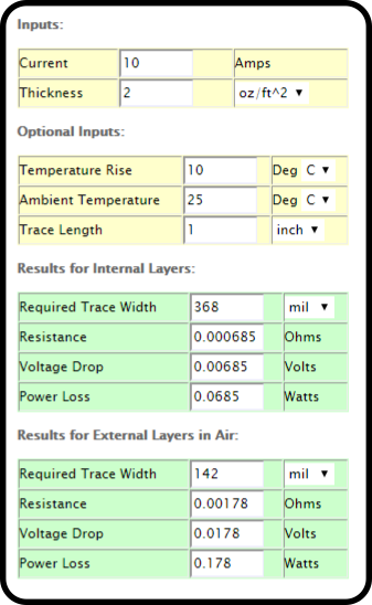
These trace width calculators will prompt you to enter design specifications such as the thickness of copper, the maximum amperage that will pass through the trace, the length of the trace, and the acceptable increase in temperature due to the resistance of the trace dissipating power. After entering these values you will be presented with a calculated trace width. It is important to note that this value is a minimum width required to meet the design criteria inputs.
Determining the width of a trace based on the current demands is important for most power traces and high-power signals, however, most traces on PCBs pass signals which draw negligible current. For these low-power signal traces, we must look at other characteristics of the PCB to determine the width.
Trace Spacing
The size of a PCB is directly connected to the cost of the PCB, so in general, PCBs are kept as small as possible. The downside of reducing board size is that it can limit the available space to route traces. For low-power signal traces, it is generally advised to keep traces small to increase the available space available for routing. Excessively large traces consume valuable PCB space while offering highly diminished returns. 6 to 30 mils are typical for most signal trace widths.
MacroFab offers a minimum of 5mil traces as a standard and if smaller traces are required, the extended manufacturing option will allow traces all the way down to 3mil.
Read about the dangers of too-narrow trace widths now.
Trace Termination
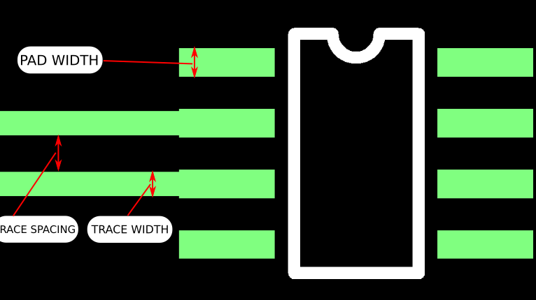
The point at which a copper trace meets a pad can also inform the width of a trace. In most cases, trace widths are set to the same width as the pad they terminate to. This will help aid with routing traces away from the component they connect to and will avoid violating spacing between adjacent traces. The image here demonstrates this.
In the image, we can see two traces stemming from the SOIC-style footprint. The width of these traces is slightly smaller than the width of the component pads. This allows for plenty of clearance between adjacent pads while routing away from the chip.
Selecting trace widths for BGA components can be more tricky. Read more about best practices for BGA pad creation and methods of routing traces from BGA footprints.