Sales

Weekdays:
8:30 AM - 5:30 PM CDT

832-564-0638

Support

Weekdays:
8:30 AM - 5:30 PM CDT

832-924-0146

Image 1 1447177221379

MacroFab Blog

Handling Silkscreen Over Component Pads

Published on November 10, 2015
Written by The MacroFab Team
Related Topics
PCBA Design: Five Tips to Clean Up Your Layout

Before sending your final design files to the CM for PCB manufacturing, check out these useful tips and final steps.

Top 10 Causes of Magic Smoke

Magic smoke is produced by severe electrical over-stress of your circuits and components. Here are the main causes, and how to avoid them.

Solving Procurement Challenges for Your PCB Assembly

Curious how to resolve issues you may be having with your PCB assembly process? Read our guide to see how MacroFab can help!

Other Resources

MacroFab Engineering Podcast
Blog
eBooks & Guides
Webinars
Videos
Case Studies
MacroFab Platform Help

One of the issues commonly seen in PCB design is silkscreen information overlapping exposed copper on pads. If the ink from the silkscreening process is on a pad that is to be soldered it will likely inhibit the solder from flowing and will result in a bad joint. In general, it is a good idea to never have silkscreen on any exposed copper that is to have solder applied.

When the gerber files are sent to a board manufacturer they are typically reviewed for issues including silkscreen on pad. In most cases the manufacturer will adjust the gerber information to prevent this by removing or moving the overlapping information. Although these issues are typically caught it is not good design practice to rely on it.

In some cases, the manufacturers will not make changes and create a board that has the issues (They make the board exactly as the gerber files tell them).

Luckily, fixing silkscreen over component pads with EDA tools is simple. Getting into the habit of creating component footprints with no silkscreen over component pads is worthwhile and prevents issues in manufacturing.

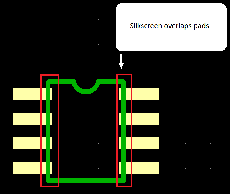
The following picture shows a SOIC-8 package where the pad width was selected to be too long. The red boxes around show areas where the silkscreen (green in this example) overlaps the pads.

Image 1 1447177221379

Image 1 1447177221379

The solution to this issue would be to reduce the width of the pads or move them further out from body of the component. In the following image the pads were moved from the body such that there is 0.01″ of space between the silkscreen and pad.

Image 2 1447177233459

Image 2 1447177233459

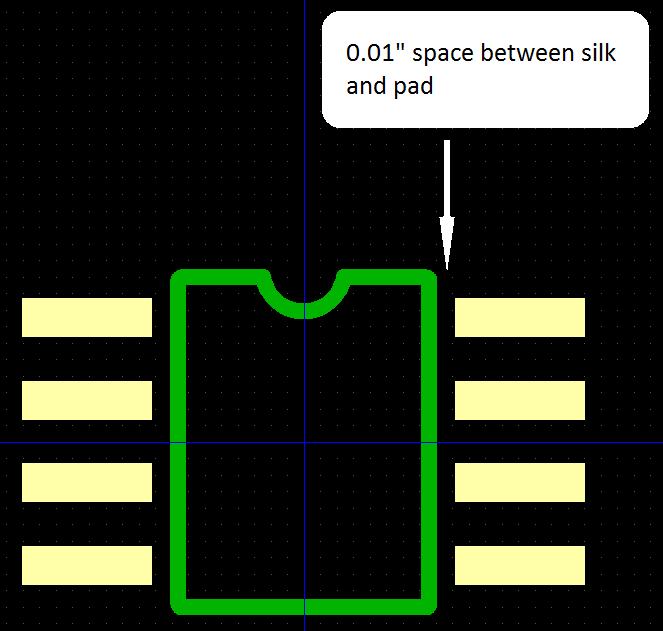
0.01″ (10mils) is a good general number for spacing between silk and copper to prevent issues.

There are cases where the designer wants information such as dimensions and assembly information to appear on the board in their EDA tool. The following picture shows an example of dimension lines crossing into pads.

Documentationlayerexample 1447177246063

When adding such information, it is important to not use the silkcreen layer. In this case, the dimension layer 48 in Eagle was used to draw the dimension lines. The information on this layer is not included in the exported gerber files that are sent to the PCB manufacturer and will not show up on the silkscreen.

Making sure that pads and exposed copper is free from silkscreen is good design practice and prevents manufacturing issues.

Related Blog Posts

BOM Management 13

Solving Procurement Challenges for Your PCB Assembly

Curious how to resolve issues you may be having with your PCB assembly process? Read our guide to see how MacroFab can help!

Screen Shot 2019 11 04 at 1

Top 10 Causes of Magic Smoke

Magic smoke is produced by severe electrical over-stress of your circuits and components. Here are the main causes, and how to avoid them.

Five tips to clean up your layout

PCBA Design: Five Tips to Clean Up Your Layout

Before sending your final design files to the CM for PCB manufacturing, check out these useful tips and final steps.

About MacroFab

MacroFab offers comprehensive manufacturing solutions, from your smallest prototyping orders to your largest production needs. Our factory network locations are strategically located across North America, ensuring that we have the flexibility to provide capacity when and where you need it most.

Experience the future of EMS manufacturing with our state-of-the-art technology platform and cutting-edge digital supply chain solutions. At MacroFab, we ensure that your electronics are produced faster, more efficiently, and with fewer logistic problems than ever before.

Take advantage of AI-enabled sourcing opportunities and employ expert teams who are connected through a user-friendly technology platform. Discover how streamlined electronics manufacturing can benefit your business by contacting us today.