MacroFab Blog
Updated June 12, 2024
Printed Circuit Boards (PCBs) and Printed Circuit Board Assemblies (PCBAs) are crucial components of electronics manufacturing. According to a report by Fortune Business Insights, the global electronics manufacturing services market is projected to reach $797 billion by 2029, up 58% from 2022. This stunning growth highlights its significance in modern industries around the world.
To develop useful and compelling products, it is paramount for your company to optimize PCBA manufacturing processes. However, this can be a challenging task as you must maximize efficiency and productivity across a wide range of activities. From designing the board layout to selecting the appropriate components and assembling them, every step requires precision and attention to detail. Nevertheless, by prioritizing efficient manufacturing processes, you can expect high-quality PCBAs, delivered on schedule. This can give you an edge over your competitors. With a dedication to excellence in PCBA production, you can build reliable and innovative electronics that meet evolving customer needs.
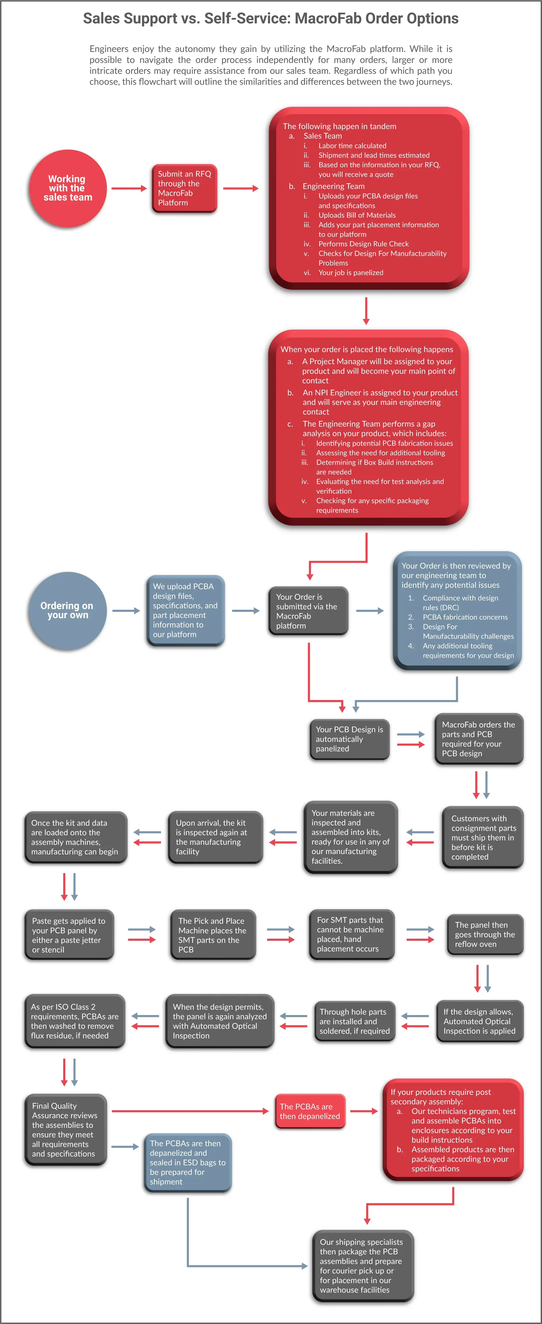
Transactional orders flowchart
Checkpoint
By identifying and addressing any issues early on, you can avoid costly manufacturing delays and rework later.

PCBA manufacturing and assembly process includes the following stages:
- Design: ideas take shape in the form of schematics and robust design files
Fabrication: digital design files take physical form on blank PCBs
Assembly: PCBs are mounted with components and gain their intended functionality
- Testing: assemblies undergo close testing to ensure proper function
- Quality Control: PCBAs are evaluated and inspected as they take shape to catch defects early
Each stage is crucial to ensure high-quality and effective electronics. However, you may encounter unique challenges and requirements along the way. To navigate these challenges, it’s important to have a thorough understanding of the process and to utilize the appropriate tools.
In this blog post, we’ll provide you with an introduction to each step and explain its significance in the larger PCB manufacturing and assembly process. We’ll also highlight relevant tools that can help you achieve your desired results. By staying informed and utilizing the latest technology, you can produce reliable and innovative electronics that meet today’s market demands.
Quick Definitions of Common Terms
What is a PCB?
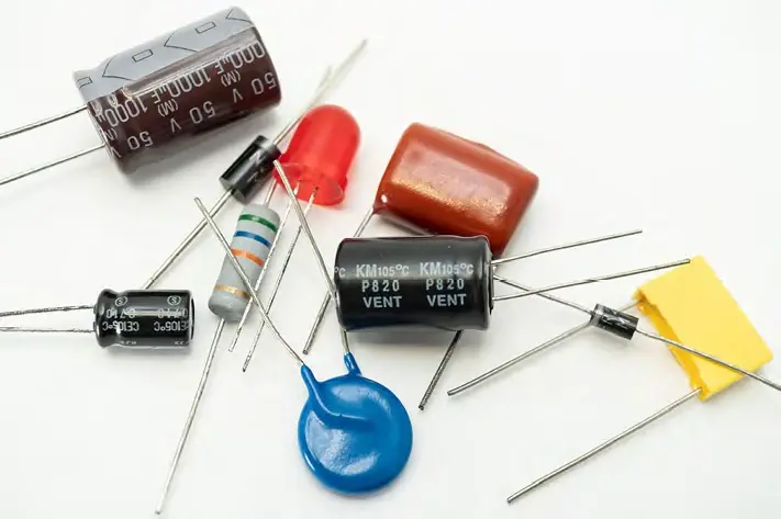
A Printed Circuit Board (PCB), or Printed Wiring Board (PWB), is made from non-conductive material with conductive copper tracks. It connects various electronic components like resistors and capacitors, enabling them to form a functional electronic circuit. PCBs are integral in almost all electronic devices, enabling the miniaturization and efficient assembly of complex circuits.You can now buy custom bare PCB boards from MacroFab.
What is a PCBA?
A PCBA, or Printed Circuit Board Assembly, is the result of soldering or assembling electronic components onto a PCB (Printed Circuit Board). This creates a fully functional printed circuit assembly, ready for use in electronic devices. The PCBA process involves attaching components like resistors, capacitors, and integrated circuits to the PCB, often through surface-mount technology (SMT) or plated through-hole (PTH) technology. Various electronic devices, from small gadgets to complex machinery, rely on PCBAs.What is the difference between a PCB and a PCBA?
While similar, PCBs and PCBAs are at different stages of production. A PCB is the board itself, designed with conductive tracks, while a PCBA includes the PCB with all electronic components, such as resistors and capacitors, fully assembled and soldered onto it.Basic Steps of PCBA Design
The design stage is where abstract ideas take shape and become ready for fabrication. As a result, it lays the foundation for all subsequent steps in manufacturing and significantly impacts production outcomes.
Below are the key steps in the PCBA design process:
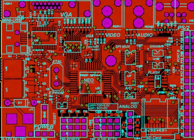
Schematic development: In this step, engineers create a blueprint for a new device that describes how electrical components are related and used on the circuit board. While it can be tempting to skip this step for simple products, schematics are absolutely necessary.
Schematic capture & synchronization: The next step is to create a new PCBA layout and “capture” the schematic, which involves arranging and linking components within a digital board representation. Utilizing schematic capture tools can accelerate this process and facilitate seamless synchronization between schematic and layout files.
PCB stackup design: PCB stackups refer to the copper arrangement and insulating layers that comprise PCBs. Stackup design is critical for minimizing impedance issues, which can affect the performance of your device.
PCBA board design rule definition: After configuring stackups, you need to define the design rules for the PCBA. Design rules set clear guidelines around object-to-object clearances, routing rules, fabrication limits, board edge clearances, and more.
Component placement: Components are then placed on the circuit board, either automatically with exploratory data analysis (EDA) or manually, within the design software. Proper component placement is essential for optimal device performance.
Drill hole insertion: Next comes inserting drill holes that will enable mounting and vias. The placement of drill holes may change as you iterate and route traces.
Trace routing: PCBA traces are the copper conduits that carry signal or power through the circuit board. They facilitate the connections between components that enable functionality. Accurate and precise trace routing is critical to overall device performance.
Labeling and identification: After copper traces are routed, add labels and identifiers to the board to make it easier to address errors or make design changes.
Design file generation: The final step in the design process is to generate the design files that will be used for fabrication and assembly. These files are critical for ensuring the accurate production of your PCB assembly. Necessary design files may vary depending on your contract manufacturer, but typically include Gerber/ODB++, bill of materials, and Centroid (X and Y placement) files.
By following these key steps and utilizing the latest technology and design tools, you can produce high-quality and reliable PCBAs that meet the specific needs of your electronic products.
PCBA Design Considerations
It’s important to consider manufacturing and assembly throughout the design process when building complex electronic products that contain PCBAs. You should keep the following considerations in mind to streamline the process:
First, consider component availability, lead times, and pricing data when designing new products. The more knowledgeable you are about component availability and affordability, the more resilient your designs will be. Consider these factors ahead of time to avoid potential manufacturing delays and issues.
Secondly, think ahead about testing during the design process. Consider how you can arrange components and stack-ups to make testing easier. Modern electronics development has a very narrow margin for error, so maximizing test coverage is crucial. By designing for testability, you can save time and money by identifying issues early on in the process.
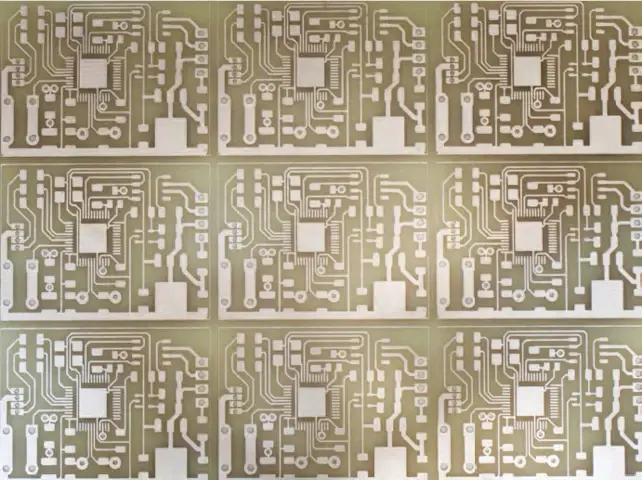
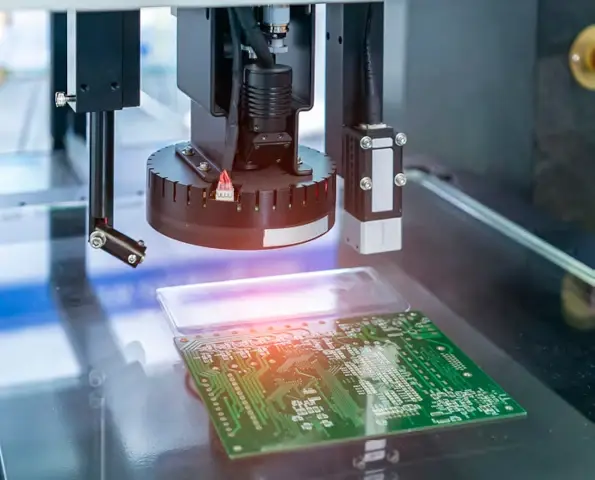
PCBA Fabrication
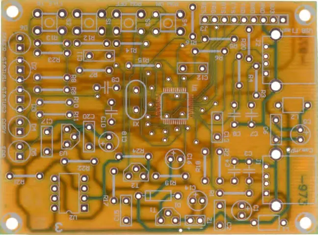
PCBA fabrication is a crucial process in electronics manufacturing, requiring high precision and attention to detail. It involves transcribing digital board designs onto physical structures through a series of carefully orchestrated steps.
The first step in PCBA fabrication is circuit image transfer. This involves the application of design data onto blank PCBs using either laser direct imaging or traditional photo tooling. Laser direct imaging is a newer technology that allows for greater accuracy and precision in the transfer process, resulting in more reliable circuit patterns.
Next comes the printing and etching stage, where engineers remove unwanted copper from the boards using chemicals to create the desired circuit patterns. The process requires great care to ensure the right amount of copper is removed, resulting in a functional circuit.
Following printing and etching, the PCB layers are bonded together through a lamination process. This ensures that electrical signals pass through proper traces and components, preventing signal interference and improving overall reliability.
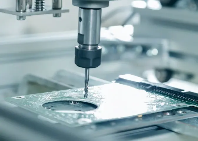
Drilling and plating are the next steps in PCB fabrication. Drilling is necessary for mounting components or creating vias for multi-layer PCBAs, while plating protects the outer PCB layers from corrosion and other environmental factors.
The final steps in the PCB fabrication process involve applying a solder mask layer and silk screening. The solder mask layer is a protective coating that prevents the PCB from oxidation and other environmental factors. Silkscreening adds labels and references to the board, such as component designators, logos, and other identifying information.
Want to know more about soldering? Read A Practical Guide to Solder Flux now.
PCB Fabrication Materials
You have flexibility when it comes to choosing materials for your PCB substrate, laminate, solder mask, and silkscreen. The three main types of materials used in PCB fabrication today are
FR-4 (glass-reinforced epoxy laminate): FR-4 is water-resistant and flame-retardant. It’s the most commonly used material in standard and high-density boards, thanks to its tensile strength and strength-to-weight ratio.
PTFE (Teflon): PTFE is a type of plastic that is best used for high-speed, microwave, and high-power
applications. The material is lightweight, flexible, and strong. It does not provide any resistance.
Metal (copper, aluminum, etc.): Metals are durable and long-lasting. They are best utilized for
applications involving excessive heat and harsh environments. They also allow companies to use
Surface Mount Technology (SMT) to integrate components.
The right choice for a given product depends on the anticipated use case, environmental factors,
and any existing manufacturing constraints.
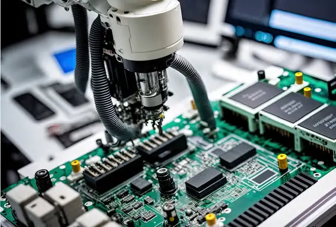
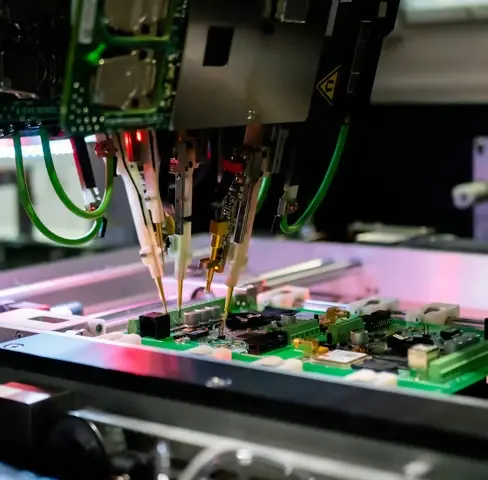
PCB Assembly
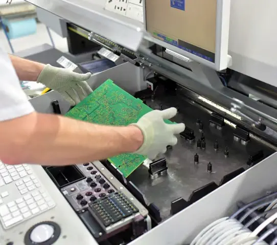
PCB assembly describes the process of mounting components onto a bare board after fabrication. The primary steps in the PCBA assembly process include:
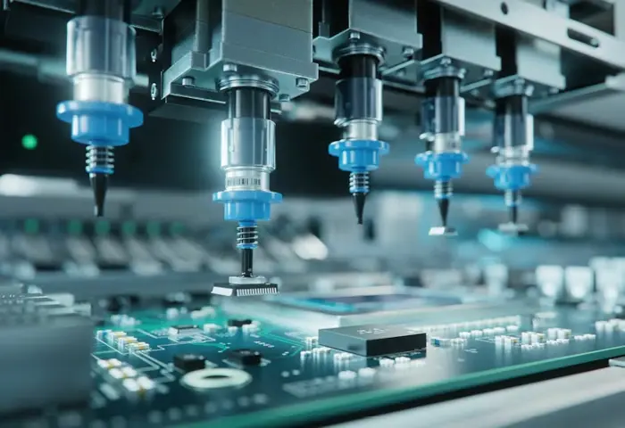
Pick and place: During the pick and place process, advanced machines use surface mount technology to place components on your fabricated PCBAs with precision and accuracy. This process allows leadless components, especially small ones, to be directly applied to the board surface for maximum efficiency. However, while SMT offers many advantages, parts can be more easily damaged or broken during installation and require specialized soldering technology and equipment.
Through-hole component insertion: PCBAs that contain components with leads or wires often must be placed using through-hole component insertion. Through-hole insertion can happen via manual soldering or wave soldering. While manual soldering can be time-consuming, wave soldering is a more automated process, but can’t be used for double-sided PCBAs. Through-hole component insertion remains a highly effective option for situations where SMT isn’t possible.
Reflow soldering: Next, if using SMT, PCBAs move through a reflow oven, which melts solder paste so that it can adhere to placed components. PCBAs then continue through coolers where the solder paste solidifies and creates a permanent connection between boards and components.
Inspection and quality control: With components soldered in place, it’s time for inspection and testing. It is important to inspect boards at this stage since soldering can lead to poor connections and misplaced components.
Read more about SMT Assembly vs. Through-Hole Assembly now.
The Benefits of PCBA Automation
It is important for modern-day PCBAs to automate the assembly process as much as possible since it accelerates production and minimizes human error, resulting in faster product delivery to meet consumer demand. Automating SMT, soldering, and post-assembly inspections is easier than ever with the right equipment and software. Automation is also less expensive per piece and more consistent when successfully implemented.
Building at scale usually requires automation, especially when using small components like surface mount components. For smaller production runs, or for those with a significant number of components that need to be inserted by hand, it may not be the most economical option.
PCBA Testing
PCBA testing is central to electronics manufacturing success. Testing mitigates risk across multiple domains. It ensures products are safe for consumers and that they meet certain quality standards.
Testing also helps reduce returns and costs related to mass production problems. Furthermore, testing enables engineering teams to improve their overall manufacturing process for future endeavors.
PCBA testing should address the following elements:
- Lamination quality: to maximize PCBA lifespan
- Copper quality: to promote proper conductivity and tensile strength
- Material solderability: to ensure components stay attached firmly to boards
- Hole wall quality: to prevent hole walls from cracking or delaminating
- Electrical leakage: to ensure electrical current can pass throughout the board
- Environmental durability: to ensure PCBAs can handle harsh environmental conditions
- Cleanliness: to ensure PCBAs don’t corrode to fail due to humidity
The most common testing methods for these components include:
In-circuit testing: In-circuit testing is the most commonly used testing method due to its speed and efficiency. With in-circuit testing, engineering teams configure a fixture with numerous sensor points that align with specific features on the board. During this process, the fixture quickly touches boards as they pass by, capturing information about what points aren’t working.
Fixtureless In-circuit testing/flying probe testing: Fixtureless testing involves holding a board in place while test pins traverse around to hit certain points. While more customizable, fixtureless testing is slower than traditional in-circuit testing. However, engineers have the ability to change test points quickly with software.
Functional circuit testing: Functional circuit testing focuses on ensuring the entire PCBA performs as intended. This testing comes toward the end of the manufacturing process and typically grades products on a pass/fail basis.
Boundary scan testing: Boundary scan testing enables engineers to test wire lines on a PCBA when it’s not possible to reach nodes via in-circuit or fixtureless testing. Boundary scan testing is especially useful for multi-layer, high-density PCBAs.
The Benefit of In-process Testing
When you are manufacturing products, in-process testing refers to the testing that occurs throughout the production process. Engineering teams will test various components and boards as they go through the different stages of PCBA fabrication and assembly. This testing can take many different forms, from visual inspections to electrical testing and functional testing.
In-process testing is essential because it allows you to catch any potential issues early in the manufacturing process before they become more significant problems down the line. This type of testing helps you identify any defects, errors, or inconsistencies in the production process that may affect the final product’s quality or performance.
In addition to improving final product quality, in-process testing can also save you significant time and money. By identifying and addressing any issues early on, you can avoid costly manufacturing delays and rework that may be required later in the manufacturing process. This can also help you reduce the risk of product recalls or returns, which can be incredibly expensive and damaging to your brand’s reputation.
Final Testing Before Shipping
When you are ready to distribute PCBAs to end users, you’ll need to conduct final testing. This type of testing provides engineering teams with a final opportunity to check certain elements and conditions, ensuring that the finished products are high-quality and reliable. In-circuit testing, which can test many aspects of board performance simultaneously, is best reserved for final testing due to its comprehensive nature.
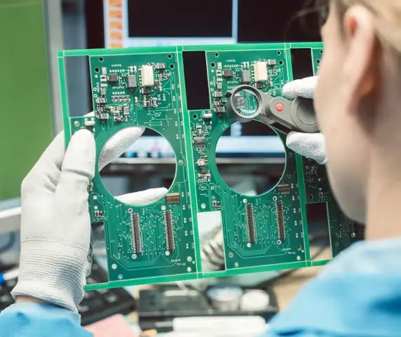
PCBA Quality Control
Similar to testing, PCBA quality control is vital for ensuring that products are safe, reliable, and effective according to their intended purpose. PCBA quality control encompasses a broad range of activities that aim to catch defects before products reach consumers. The testing described above is one form of PCBA quality control.
Electronics manufacturing can include a variety of inspections and checks, including:
Visual or microscope-based inspection: these inspections refer to having an individual, typically a person involved in assembly, check PCBAs themselves with their own eyes or with the help of a microscope.
X-Ray inspection: X-Ray inspections enable engineers to find circuit board defects that would otherwise be impossible to find via visual inspection, like solder shorts and solder bridges.
Automated Optical Inspection (AOI): AOI machines take images of PCBAs, compare them to images of ideal board configurations, and highlight any differences. Inconsistencies between the two often represent defects that require intervention. Learn more about MacroFab's AOI inspection process.
DRC checks: DRC checks make sure that schematics are viable for manufacturing. They prevent teams from moving forward with designs that aren’t feasible given certain manufacturing limitations.
PCBA Quality Control Systems
Quick issue resolution is critical in electronics manufacturing. Leveraging quality control systems is one effective way to ensure your products meet high-quality standards. These systems don’t just perform various types of testing and inspections, but they also assist in documenting any issues that arise and identifying the root causes.
Modern quality control systems offer you valuable data that can help you troubleshoot and fix problems that arise during the production process. This streamlines manufacturing and minimizes the risk of defects or malfunctions within your finished product. Additionally, documentation and data analysis features provide quality trends over time, which can allow you to make better decisions on your product design.
Following inspection, customers may choose to have their PCB assemblies mounted within an external enclosure. MacroFab offers complete box build assembly and wire harness integration options for customers who may need them.
Learn More About PCBA Manufacturing Processes
PCBA manufacturing is a long, complicated process. From design to quality control, there are many
ways that PCBA manufacturing and assembly can go wrong. Understanding each manufacturing
stage and its related tooling is invaluable.
- PCBA designs must be resilient and reflect key considerations when it comes to fabrication, assembly, and testing
- PCB fabrication must use the right materials and apply new-age image-transferring techniques whenever possible
- PCB assembly should lean on automation to minimize human error and maximize productivity
- PCBA testing has to be fast and thorough, which is easier when designs anticipate testing methods
- PCBA quality control is important up and down the manufacturing process and prevents defects as early as possible
The world is approaching $800 billion in electronics manufacturing sales, and organizations must optimize every aspect of the PCB manufacturing and assembly process if they want to compete effectively, avoid disruptions, and evolve with global demand.
Related Topics
How to Shorten PCBA Production Lead Times with MacroFab
In the rapidly evolving electronics sector, extended production lead times are no longer tolerable, and minimizing these lead times is crucial for success.
PCBA Order Lead Time Report: Guidance for Lunar New Year 2025
With Lunar New Year coming up, MacroFab wants to ensure they give the best guidance when planning orders to continue meeting delivery guidelines.
Designing Rugged PCBAs for Smart City Applications
PCBA design in smart city applications have become a staple in making a change. From instances such as smart electric grids, crime detection, and waste.
Download the Step-by-Step Guide to PCBA Production
Learn how MacroFab can assist with your PCBA mass production needs.
About MacroFab
MacroFab offers comprehensive manufacturing solutions, from your smallest prototyping orders to your largest production needs. Our factory network locations are strategically located across North America, ensuring that we have the flexibility to provide capacity when and where you need it most.
Experience the future of EMS manufacturing with our state-of-the-art technology platform and cutting-edge digital supply chain solutions. At MacroFab, we ensure that your electronics are produced faster, more efficiently, and with fewer logistic problems than ever before.
Take advantage of AI-enabled sourcing opportunities and employ expert teams who are connected through a user-friendly technology platform. Discover how streamlined electronics manufacturing can benefit your business by contacting us today.