Dealing with Common PCBA Design Errors and How to Avoid Them
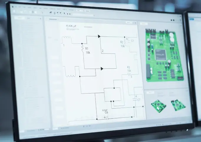
As with product development in any industry, electronics manufacturing begins with the design phase. Printed Circuit Board Assembly (PCBA) design refers to developing Printed Circuit Board (PCB) schematics and design files that will eventually become physical products.
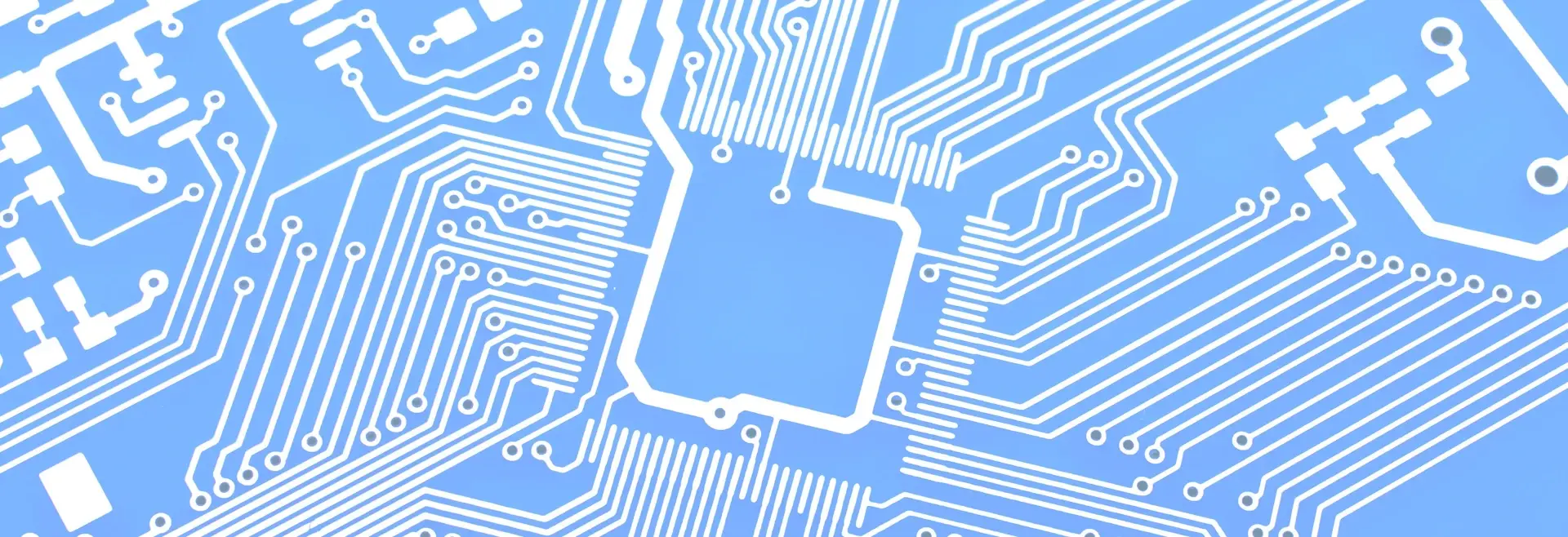
PCBs are blank circuit boards that will soon contain integrated circuits and components. PCBAs refer to the fully assembled board, including the PCB and the components required for the board to fulfill its purpose.
With the increasing need for critical applications technology, PCBAs have become smaller and more complex, requiring designers to create more individual designs in a shorter time frame. As a result, creating clean designs has become more challenging.
PCBA design has a significant impact on manufacturing outcomes, determining which assembly techniques will be used. Therefore, it’s crucial to get PCBA design right, and teams must pay close attention to their design approach. Engineers can mitigate huge risks and problems when they do.
This post will cover the most common errors that occur during custom PCBA design, including misaligned components, unrouted signals, and overheating components. To maximize manufacturing productivity, design engineers need to know and understand the available PCB design tools so they can avoid, identify, and fix such errors as early as possible.
Checkpoint
With the increasing need for critical applications technology, PCBAs have become smaller and more complex, requiring designers to create more individual designs in a shorter time frame.

Key Takeaways
• PCBA design is critical for successful electronics manufacturing and requires careful attention to detail.
• DFM guidelines can help avoid routing errors, such as avoiding sharp angles, minimizing the use of vias, and using standard trace widths.
• Best practices for avoiding power distribution errors include properly sizing the power supply, optimizing power distribution network designs, and using electrical power system analysis software or power integrity analyzers to estimate power quality.
• Thermal management is critical, and engineers must be aware of their primary heat sources, incorporate heat sinks, and use thermal analysis software.
• Airflow, thermal vias, and power delivery networks can also impact thermal management.
Types of PCB Design Errors
To tackle custom PCBA design errors, engineers need to familiarize themselves with the most prevalent issues that may arise nowadays. Over the years, the challenges they face have evolved due to improvements in manufacturing technology and higher consumer expectations.
In modern electronics development, the primary types of PCBA design errors include:
- Component placement errors
- Routing errors
- Power distribution errors
- Thermal management errors
Each error can impact the PCBA manufacturing process in various ways, and some errors may be more serious than others. However, it’s crucial to address all as soon as possible. Here, we will provide an overview of these errors and explain how they can affect PCBA quality.
Component Placement Errors
There are different types of component placement errors that can occur during PCBA design. Misaligned components are one such error, which can result in functionality and reliability problems. As PCBAs become smaller and denser, engineers may feel pressure to optimize board space, which can lead to improper component alignment.
It’s also crucial to leave adequate space between components, board features, and board edges. Failing to do so can make it difficult to test nodes in an automated manner. Additionally, designs with high-speed parts may experience signal integrity and excess heat issues if not strategically positioned on the board.
Another error occurs when engineers place components in the wrong orientation. Proper component orientation is critical to ensure current flows in the correct direction. Engineers may make this mistake because they overlook which components are polarized or neglect to consider orientation during design.
Such errors can become costly and require significant time to correct. Identifying and resolving component placement errors early in the design process can prevent delays and avoid additional expenses during the manufacturing stage.
Best Practices for Avoiding Component Placement Errors
To ensure proper component placement, engineers must align, space, and orient components correctly. If possible, similar component packages should be grouped together and oriented consistently, even if it takes up more space. This will make assembly and testing easier.
Regarding spacing, engineers should mind design rule checks (DRCs) and spacing best practices for all component types. Do not place components near areas that generate heat or that interfere with trace routing. Advanced software design tools can simplify this process by providing thorough design for manufacturing (DFM) checks and helping engineers follow placement guidelines from the contract manufacturer.
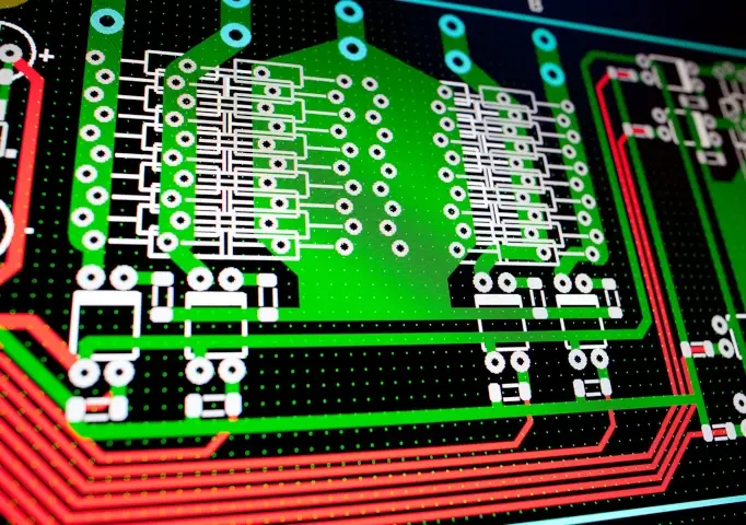
Routing Errors
PCBA design can result in two primary routing errors: unrouted signals and shorted circuits.
Unrouted signals occur when the connections between components are incomplete, resulting in open circuits. This can cause the PCBA to malfunction and lead to issues like abnormal heat retention, impedance mismatches, and unusual circuit behavior. With the growing PCBA design complexity, it’s easy for engineers to lose track of their routes.
Shorted circuits are another common issue in PCBA design. They can happen for the same reason as unrouted signals, where a hot wire inadvertently extends current to another conductor. This can cause signals to deviate from their intended path on the board, leading to erratic performance.
Other possible issues related to routing errors include:
- Crosstalk: This occurs when the signals from one trace interfere with another trace due to their proximity, leading to signal degradation or noise. To avoid crosstalk, it’s important to maintain adequate spacing between traces and to use ground planes or shielding if necessary.
- Impedance matching: This is crucial for high-speed signals to ensure they propagate correctly without reflections. When the trace impedance is not matched to the driver and receiver, it can lead to signal distortion, timing issues, and reduced signal integrity.
- Signal integrity: This refers to the ability of the circuit to transmit signals without distortion or loss. Routing errors can compromise signal integrity and cause issues like jitter, noise, or reduced voltage swings.
It’s important to keep DFM guidelines in mind when designing the printed circuit board layout, as it can help avoid routing errors leading to manufacturing issues. For example, avoiding sharp angles, minimizing the use of vias, and using standard trace widths can improve design manufacturability. By keeping these factors in mind, engineers can avoid common routing errors and improve the performance and reliability of their PCBAs.
Best Practices for Avoiding Routing Errors
To prevent routing errors, engineers can take several steps. Firstly, teams can use design and simulation tools to detect unrouted signals and verify correct routing. Advanced platforms keep track of all electrical connections specified in a schematic, ensuring that everything is wired up correctly and that routes don’t generate crosstalk or interference.
Ground routing is another important factor in preventing routing errors. Engineers need to design the ground plane carefully, taking voltage return, signal return, noise, and interference into account. PCBA simulation software provides the necessary data and functionality to configure ground planes and identify routing problems easily. In PCBAs with many routes, simulation tools are particularly important.
Power Distribution Errors

Power distribution errors typically involve an overloaded power supply and inconsistent voltage levels. Overloaded PCBs occur when too much current passes through the board, often due to a lack of insight into critical power metrics by electronics engineers. Overloaded PCBAs tend to overheat, which can damage the board.
Inconsistent voltage refers to power fluctuations beyond expected levels within the power delivery network, leading to false responses and unexpected PCB behavior. The problem here is limited visibility into how voltage moves throughout the board and where levels might be inconsistent.
Ultimately, both power distribution errors result from uninformed power delivery network (PDN) design. PCBs have become more complex, so configuring a PDN that consistently distributes power to all components while avoiding unnecessary noise and tolerance is difficult.
Best Practices for Avoiding Power Distribution Errors
To solve power distribution errors, engineers need to properly size the power supply and optimize power distribution network designs. Managing the power supply involves following power distribution best practices, such as selecting the appropriate regulator, implementing EMI filtering, and using decoupling capacitors. The specific method of implementing the right power supply depends on the application and components involved in the design.
To optimize the PDN, engineers should use electrical power system analysis software or power integrity analyzers that estimate power quality and provide insight into voltage drops or hotspots across the board. With this information, engineers can make more informed decisions and prevent power distribution errors before fabrication.
Thermal management, grounding, trace impedance, and power plane design are all essential to preventing power distribution errors on PCBAs. Components should be spaced out correctly, and the ground plane should have low impedance and low inductance. Low impedance and wider traces can help reduce voltage drops and noise. Power planes can provide a low-impedance path for power distribution, but the proper design is crucial to avoid potential issues.
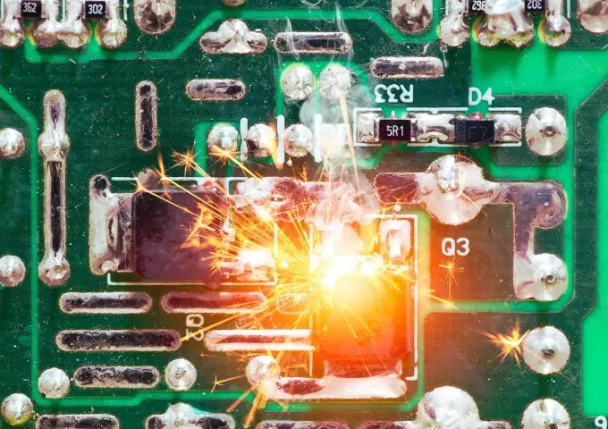
Thermal Management Errors
Many engineers struggle to manage PCBA thermal characteristics. As previously mentioned, increasing component density on boards means tighter spaces, which can lead to overheating if thermal management is not carefully considered.
High heat can stem from components malfunctioning or when distances between surface mount devices (SMDs) are too wide. If certain components malfunction, others may have to produce more power to compensate, leading to excess heat. This can also occur when SMD placements are too long, generating excessive heat. High-frequency circuits already generate more power, further increasing the likelihood of overheating.
When components get too hot, the integrity of the board is compromised. Excessive heat can cause PCB layers to expand, warp, and separate. It can also damage circuit lines and cause PCBA components to oxidize. These issues occur when engineers fail to dissipate heat properly or use the wrong materials for their applications.
Best Practices for Avoiding Thermal Management Errors
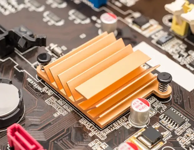
To avoid thermal management errors in PCBAs, good thermal management system design and strategic component placement are necessary. If the PCBAs have hot components, engineers should incorporate heat sinks and cooling devices to minimize excess heat. Heat-resistant materials like FR-4 are also essential for high-temperature applications.
To prevent thermal management issues, engineers need to be aware of their primary heat sources, typically microprocessors and microcontrollers. Temperature sensors placed near thermally active components can provide engineers with an accurate sense of board temperature.
Optimal component placement is also critical for thermal management. Engineers should place components at optimal distances to balance power distribution across the board, reducing the likelihood of some components having to step up due to power generation limitations. Wider traces can help dissipate heat into the air and eliminate heat spots.
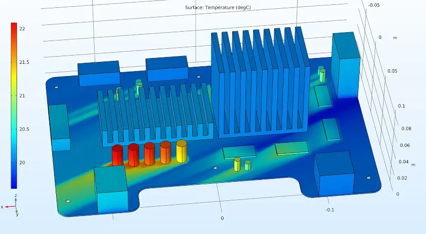
PCBA thermal analysis software is a valuable tool for thermal management. Engineers can analyze how temperature is distributed across their designs and identify areas with potential deformation. Some tools also show how heat spreads throughout the board due to airflow, providing designers with insight into ideal fan placement. With this information, PCBA thermal management becomes less daunting.
In addition, keep these points in mind when planning for thermal management:
- Airflow: Good airflow is critical for thermal management. Engineers should design PCBAs with sufficient clearance around components to allow for proper airflow, and they should also consider the placement of fans or other cooling devices.
- Thermal vias: Thermal vias are small holes in the PCB that connect the copper traces on the top and bottom layers, providing a low-impedance path for heat flow. Engineers should place thermal vias close to thermally active components to help dissipate heat.
- Power delivery network: The power delivery network can also impact thermal management. A poorly designed PDN can result in excess heat, so engineers should design the PDN with low impedance and proper capacitance to reduce voltage ripple and power losses.
- Simulation: Simulation tools can help engineers optimize thermal management in their designs. With thermal analysis software, engineers can model and simulate different scenarios to identify potential hot spots and optimize cooling strategies.
By considering these factors and implementing appropriate design practices and tools, engineers can prevent thermal management issues and ensure reliable PCB designs.
Learn More About Avoiding PCB Design Errors
This blog post is a starting point for how to address the biggest custom PCBA design errors that engineers face today. Component placement errors, routing errors, power distribution errors, and thermal management errors can all threaten PCBA manufacturing. When these errors sneak through the design phase, engineering teams spend more time and money backtracking before they can move forward with fabrication and assembly. This can’t happen in today’s hypercompetitive, fast-moving electronics sector.
The good news is that design software and simulation tools exist that make each error type described here easier to spot. Modern software solutions can:
Review how components are placed based on DRCs and guide engineers to use proper orientation, spacing, and alignment
Identify routing errors, like unrouted signals and open circuits, as well as run simulations that give engineers an accurate sense of how current moves throughout their boards
Support power delivery network design to ensure that electrical signals are consistent and reliable as they travel from component to component
Estimate temperatures across the PCBA and show how temperature differs based on the heat sink and cooling fan placement
Follow the best practices summarized here, and adopt new design tools if any errors are hurting your electronics development process. Addressing custom PCBA design errors early is the key to producing high-quality, reliable electronics at scale.
To go deeper into PCBA design principles, download MacroFab's 75-page eBook Engineering Design Essentials: The PCBA Design Handbook.
Related Topics
Struggling with Inflexible PCB Assembly? MacroFab's Got Your Back.
Many electronics designers struggle with systems that demand complete data and specific formats upfront. Wouldn't it be great if there was a better way?
Fab Insights: HASL vs ENIG
Choosing the right surface finish for a PCBA can be tricky. HASL and ENIG differ in their methods of coating printed circuit boards.
How Do QFN Packages Compare to Other Surface Mount ICs?
This article aims to arm electrical engineers and PCBA designers with comprehensive insights into the QFN package.
Build from anywhere, anytime, with MacroFab.
Order OnlineAbout MacroFab
MacroFab offers comprehensive manufacturing solutions, from your smallest prototyping orders to your largest production needs. Our factory network locations are strategically located across North America, ensuring that we have the flexibility to provide capacity when and where you need it most.
Experience the future of EMS manufacturing with our state-of-the-art technology platform and cutting-edge digital supply chain solutions. At MacroFab, we ensure that your electronics are produced faster, more efficiently, and with fewer logistic problems than ever before.
Take advantage of AI-enabled sourcing opportunities and employ expert teams who are connected through a user-friendly technology platform. Discover how streamlined electronics manufacturing can benefit your business by contacting us today.