During the PCBA production process, solder joints play a crucial role. Surface mount technology (SMT) assembly relies heavily on the quality of the solder paste deposit. This sensitive process requires careful application during the solder paste printing process to ensure robust electrical connections.
SMT processes have made significant improvements in recent years, leading to improved efficiency, accuracy, and reliability. In this article, we will explore the latest innovations in solder paste printing technology and their impact on the electronics manufacturing industry.
The Importance of Solder Paste Printing
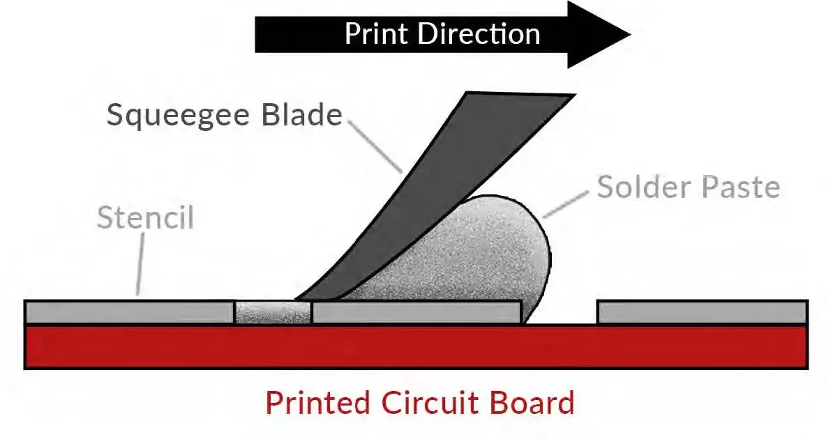
Solder paste printing requires a complex mix of solder alloy and flux. It can be difficult to print on bare SMT boards due to the need for clean, regular surfaces. Stencils should be aligned, solder paste must have the right viscosity, and stencil design must be free from imperfections.
Additionally, since modern SMT boards use finer pitch components placed closer together, bridges are more likely to form (solder connecting adjacent pads). Addressing such challenges requires careful process control, expertise, and attention.
Before diving into the innovations, let’s first understand why solder paste printing is a critical step in the SMT process.
Creating Accurate Solder Deposits
Solder paste printing is responsible for creating accurate and consistent solder deposits on the PCB assembly. These deposits are crucial for ensuring proper electrical connections between components, which is essential for the functionality and reliability of the final product.
Solder paste printing provides consistent quality across high-throughput, reducing assembly errors and inefficiencies to provide higher overall yields.
Accurate solder deposits make sure each SMT component connects to the board exactly where intended–particularly important for high-density boards. It also directly affects electrical connectivity between components and the entire PCB.
Moreover, accurate solder deposits have an outsized impact on thermal management, as adequate solder volume aids in dissipating heat effectively and keeps the board at an optimal temperature.
Cost and Time Savings
Solder paste printing is also a cost and time-saving process. It allows for the simultaneous printing of multiple PCBs, reducing the time and labor required for manual soldering.
Most importantly, solder paste printing provides consistent quality across high-throughput, reducing assembly errors and inefficiencies to provide higher overall yields. Consistency is key. With the controlled and repeatable nature of solder paste printing technology, quality increases.
Flashback: Listen to the day MacroFab got a new automatic screen-printer.
Innovations in Solder Paste Printing Technology
Now, let’s take a look at some of the latest innovations in solder paste printing technology and how they are revolutionizing the electronics manufacturing industry.
3D Solder Paste Inspection (SPI)
One of the most significant advancements in solder paste printing technology is the integration of 3D solder paste inspection (SPI) systems. A laser or structured light system uses three-dimensional images to ensure accuracy and consistency in solder paste deposits.
SPI systems use 3D imaging to capture the height, volume, and shape of the solder paste deposits, providing a more comprehensive inspection than traditional 2D systems. This can detect defects such as insufficient or excess solder, bridging, and misalignment, affecting the final product’s reliability.
By catching these defects early on, SPI systems reduce the need for rework and improve the overall quality of the PCBs.
Automatic Solder Mask Inspection (ASM)
Another innovation in solder paste printing technology is the integration of automatic solder mask inspection (ASM) systems. To detect minute defects on the solder mask layer, ASM systems use high-resolution cameras and sophisticated lighting techniques.
It detects defects such as misalignment, insufficient solder masks, and contamination in 2D and 3D. By catching these defects early on, ASM systems improve paste accuracy and consistency and improve the overall quality of the PCB.
Automated Solder Paste Printing
As technology has advanced, automated solder paste printing has become a reality, replacing the manual process of stenciling solder paste onto PCBs.
Automated solder paste printing machines use advanced vision systems and robotics to accurately and consistently deposit solder paste onto the PCB. These machines can also adjust for variations in the PCB and stencil, resulting in precise and consistent soldering.
By automating this process, manufacturers significantly increase their production speed and reduce the risk of human error, resulting in improved efficiency.
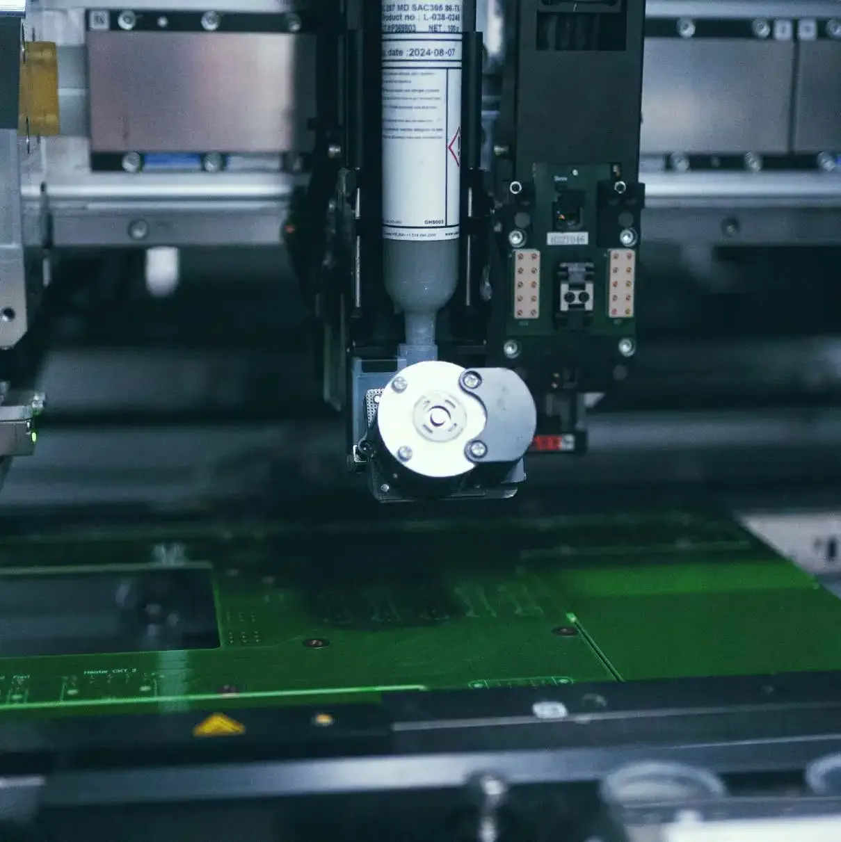
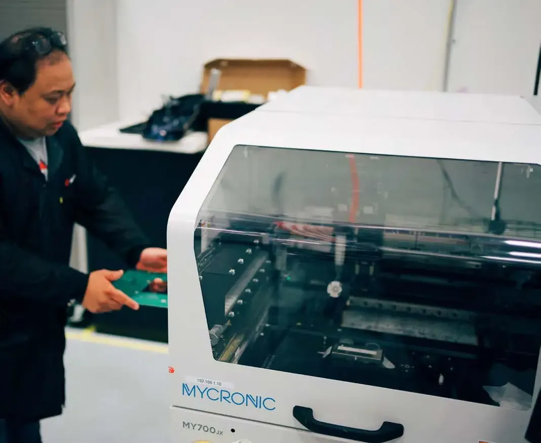
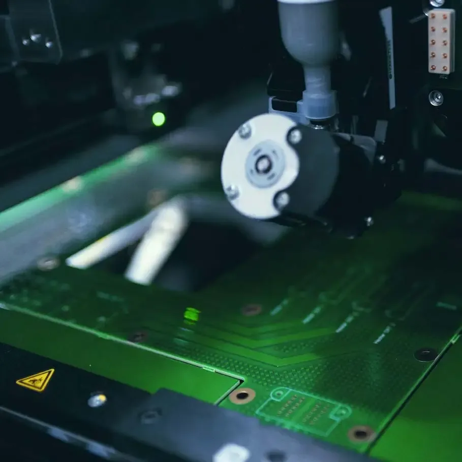
MacroFab uses the latest technology to deliver exceptional quality and fast turnaround. We’ve invested in the MY700JX solder paste jetting machines from Mycronic. This particular machine offers superior precision with non-contact jetting, even for fine-pitch components. With speeds of over 1 million dots per hour, it also reduces production times.
Need more help with your soldering project? Learn what solder flux is for and how to use it effectively.
Nano-Coating Technology
Nano-coating technology is another innovation that is transforming the solder paste printing process. This technology involves applying a thin layer of a hydrophobic coating to the stencil, which repels the solder paste and prevents it from sticking to the stencil.
This coating allows for a more consistent and accurate deposition of the solder paste, reducing the risk of bridging and other defects. Additionally, it reduces the need for frequent stencil cleaning, saving time and improving efficiency.
Smart Stencils
Smart stencils are another innovation that is changing the game in solder paste printing. The stencils contain sensors that can detect pressure and temperature during the printing process, providing real-time feedback to the machine. Smart stencils also have a longer lifespan than traditional stencils. This reduces the need for frequent replacements and saves money.
The Future of Solder Paste Printing
With the continuous advancements in technology, the future of solder paste printing looks promising. Here are some potential developments that we can expect to see in the coming years.
Artificial Intelligence (AI) Integration
The integration of AI in solder paste printing is a possibility that could revolutionize the process even further. AI algorithms could analyze data from SPI and ASM systems to identify patterns and predict potential defects, allowing for proactive measures to be taken to prevent them.
Additionally, artificial intelligence could help optimize printing processes, offering greater flexibility in dealing with diverse PCBA designs and quick changes. Moreover, a real-time AI calibration could improve solder paste deposits by compensating for variations in the PCB and stencil.
3D Printing of Solder Paste
Another potential development involves 3D printing technology to deposit solder paste onto the PCB. This could eliminate stencils and allow for more complex and precise solder deposits.
3D printing could also be used to create custom stencils for each PCB, further improving accuracy and consistency.
Conclusion
Solder paste printing technology has come a long way in recent years, and the advancements we have seen are just the beginning. With the integration of 3D SPI and ASM systems, automated printing machines, nano-coating technology, and smart stencils, the process has become more efficient, accurate, and reliable.
As technology continues to evolve, we can expect to see even more innovations in solder paste printing, leading to improved efficiency, cost savings, and higher-quality PCBs.
Get an Instant Quote from Your Design or Specification Files.