Plated slots are plated through-hole pads with a non-circular shape.
Most through-hole components in PCBs have circular or square leads which fit nicely in circular holes, but what happens when you have a component that has non-circular or square pads? For example, let’s take a look at the 2.1 mm DC jack made by Switchcraft (Part Number: RAPC722X).
This part has three leads each of which is rectangular in shape. Here is a snapshot from the datasheet of the DC jack dimensions:
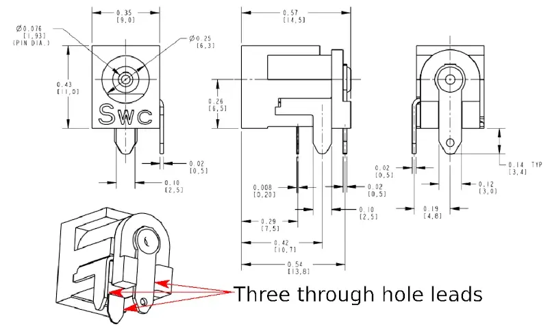
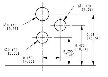
The three leads on this device are thin and wide rectangular shapes that can be soldered into a circular hole but this is not the most ideal solution. Let’s take a look at why. Here is a picture of the recommended footprint for using circular through-hole pads from the datasheet.
If we take that information and make a footprint in our EDA tool we can get a better idea of how it will look.
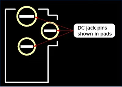
In general, this footprint appears to be acceptable, but check out what happens when we superimpose the outline of the DC jacks lead size in the circular pads that we just created.

Since the hole in the pad needs to have a diameter wide enough for the pin to fit through we are left with a lot of open space from the pin to the copper on the edge of the hole. In the next image, the open space is highlighted blue to demonstrate this.

When to Use Plated Slots
The reason this method is non-ideal has to do with the soldering process. The open space shown in the image above will have to be filled with solder when building the board. Since this open space is significant, a lot of solder will be required to bridge the gap.
Electrically there are no issues with this style of component mounting, but consider the case if you wanted to mount other components that had wider leads. At some point, the hole would be too large to fill with solder becoming non-practical. PCB mounting pins such as the ones on the DC jack in circular holes work well, but we need a better method for mounting larger and odd shape pins. Using large circular holes is not well suited for layouts requiring tight size constraints or dense component population.
Luckily, we have the capability to manufacture plated slots that are non-circular in shape and can accept pins such as the ones on the DC jack with much less open space to solder. Let’s take a look at how to do this.
How to Create Plated Slots
To create a plated through-hole we have to define a few things in our EDA tools. For most EDA tools, plated through holes are created through a manual process where the designer specifies all the aspects of the hole as opposed to simply placing a standard pad. There are three things to consider when creating a plated through hole: the shape of the copper on the top layer, the shape of the copper on the bottom layer, and the shape of the hole.
The following is a rendering of a PCB with a plated through-hole which give an idea of the items that need to be defined in the design tools.
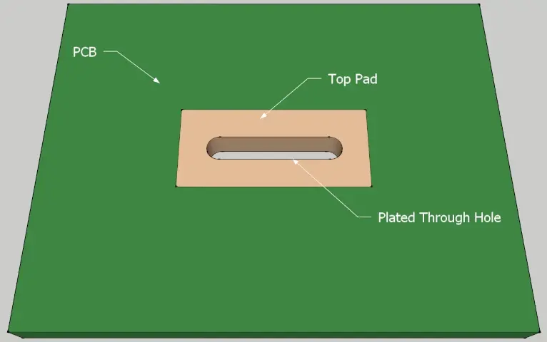
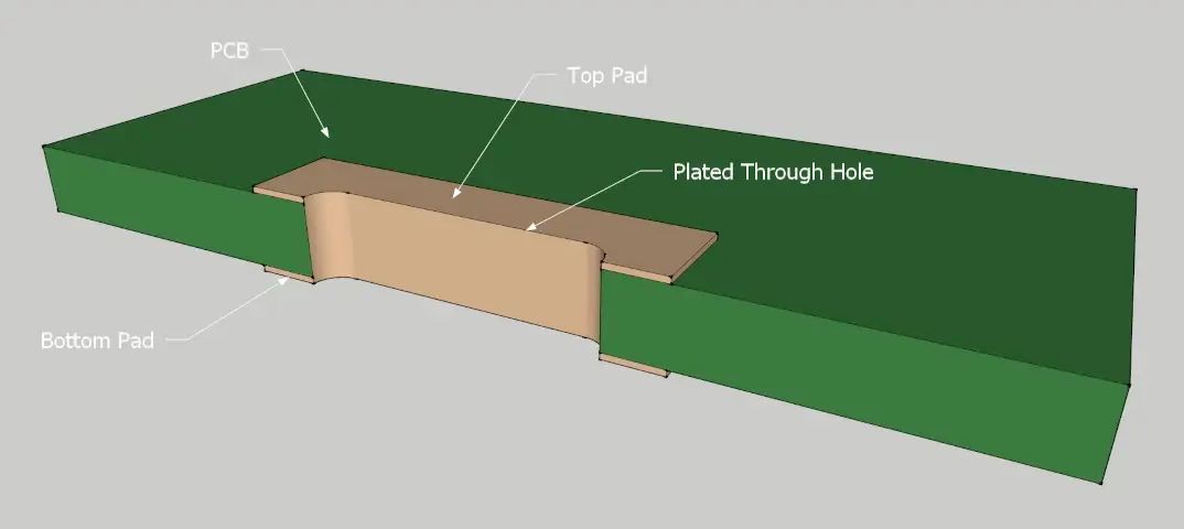
And here is a cross-section cut of the same pad. To create a plated through-hole such as this we start by placing a pad on both the top and bottom layers to create the top and bottom copper. These pads can actually be SMD rectangular style pads or they can simply be shapes drawn directly on the top and bottom copper layers. It is critical that both the top and bottom pads are larger than the hole. It is not necessary for both the top and bottom pads to be identical, but in most situations, they will be.
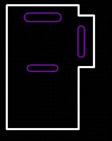
Here is a footprint of the DC jack from earlier with SMD rectangular pads on both the top and bottom layers.
The bottom pads are not visible in this image because they were created to be identical in size and shape to the top. Now that the pads have been defined, we need to add the holes.
Plated through-holes differ from most other holes in PCB design as they are not included in the standard drill file, instead they are drawn on the board outline layer. When manufacturing files are sent to a PCB manufacturer, the board outline is interpreted as cutting information. If a shape exists on the board outline layer, the PCB manufacturer will route the board inside the shape that has been drawn. If a hole is drawn inside pads that are on the top and bottom of a PCB, the board manufacturer will interpret this as a plated through-hole.

Knowing this, we need to draw the holes we wish to have in our footprint on the board outline layer. In the following image, I have shown the footprint from above with the cutouts shown as purple slots. The pads are not shown for clarity.
That’s all it takes to make a plated through-hole. When generating the manufacturing files, the pads will exist on the top and bottom layers and the slot will appear on the board outline file.
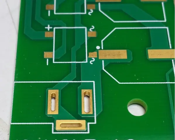
Here is a picture of a board that was recently manufactured with this footprint.
To recap, making plated through holes is as simple as creating pads on the top and bottom layer and defining a hole on the board outline layer. Plated holes allow designers to use parts with non-circular leads and pins while maintaining good electrical and mechanical connections. With a little creativity, even components such as panel mount potentiometers can be mounted to a PCB using plated holes.
Find out more about placing components with our footprint files blog posts.