Introduction to EMC Compliance in PCB Design
If you’re new to EMC compliance, you may find the process daunting. Most commercial printed circuit boards used for consumer products will require FCC certification for use in the USA. Acceptance is also required by European Directive for use in Europe with other international regions having similar testing.
Electromagnetic compatibility (EMC) from a transmission point of view is the unintentional generation, propagation and reception of electromagnetic energy (RF signals) which may cause unwanted effects such as electromagnetic interference (EMI) in other systems. From a receiver point of view, it is the ability of equipment or a system to satisfactorily operate in a normal electromagnetic environment in the presence of other potential interference.
Without these standards in place, your Wi-Fi (IEEE 802.11) may cease to work alongside Bluetooth radios (IEEE 802.15.4) and also in the presence of your microwave oven. All of these operate within the same 2.40 – 2.48GHz ISM frequency band. The ISM band is a license-free band used for Industrial, Scientific and Medical applications. Due to the wide use of this frequency band, it has become congested will a multitude of applications. Although EMC testing may be concerned with any spectrum interference, the ubiquitous proliferation of applications in the ISM band within electronics makes these frequencies especially important to test for.
Issue Classes for Testing
EMC testing involves the pursuit of three main issue classes. These include:
- Emission of spectral radiation
- The susceptibility of a system to be encumbered by interference
- Coupling of one system inadvertently to another.
For a non-wireless system, it is especially important to test for non-intentional radiation effects. Non-intentional radiator opportunities exist for EMC emissions within PCB and wired communications when an RF signal is emitted without transmission intent, due to the design of the system. Intentional radiators are systems that use intentional RF/Wireless signaling to get information onto and off the board. EMC compliance testing ensures that these intentional signals stay within certain bandwidths and power requirements for the application. Spectral emissions beyond these limits render a system without commercial approval.
Pre-Certified Modules
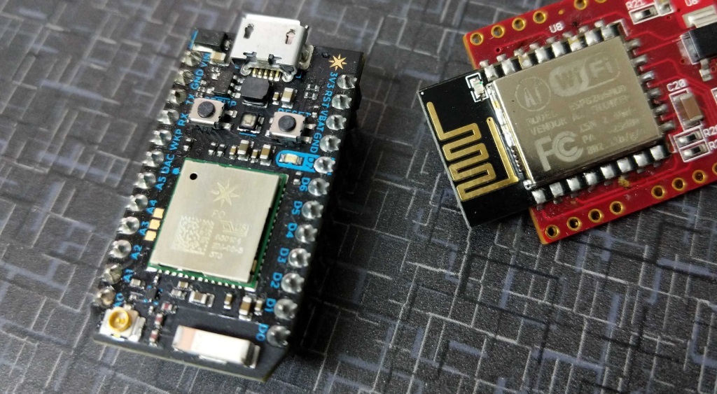
Particle ESP8266
System boards that contain an RF radio plus other complementary support circuitry can be complex to certify. One way to help simplify this challenge is to use pre-certified radio modules as the basis for the system. This ensures that the RF layout does not need to be touched or altered in any way. In addition, it guarantees that the signal power, bandwidth and channel assignments fall within the pass band of interest. Therefore, this portion of the system can be assured to pass the EMC certification. The remaining portion of the complementary circuitry will then be the focus of the testing.
There are several Bluetooth, Wi-Fi and other ISM band radio modules that are already pre-certified by the respective manufacturer. Many manufacturers may also target other specific IEEE 802.15.4 modulation schemes for unique internet of things (IoT) radios. There are other software configurable radios modules that may be certified across a broad possible spectrum. For these radios, the basic operation has been proven by the manufacturer, but the specific settings that the designer needs for their system need to be programmed into the firmware. These frequency and modulation configurations would then need to be tested uniquely to prove the radio settings.
Shielding for Your Signals
Introduction to EMC Compliance
A system that receives or transmits sensitive RF signal may need critical RF shielding to keep the signal content separated from unwanted noise coupling in the environment. In many cases, this means metals can surround a radio or antenna cabling. But, shielding can also mean keeping proper grounding paths near the RF signals.
Grounding is an important consideration for signals both to and from the antennas as well as any radio processing circuitry. The return path of a signal can be disturbed on the ground without careful attention to layout. Using buried traces within the board can be a secondary method of keeping unwanted signals from leaking into or out of the system.
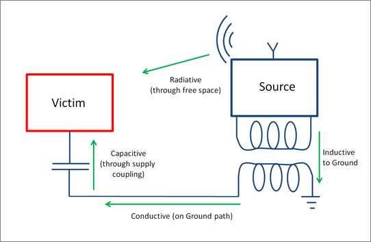
EMI Coupling
There are 4 primary electromagnetic interference (EMI) coupling modes:
- Conductive
- Inductive
- Capacitive
- Radiative
Inadvertent radiative interference occurs when a signal is transferred from a source system to a victim system by propagating through free space. The victim system can be adversely impacted if it is forced to accept this radiative signal. Similarly, interference from the source can couple through inductive means to a ground plane or shared control lines. A corrupted ground path can impact all other circuits that rely on this ground to be a clean signal. A capacitive interference may occur on a supply line that is coupled to ground with bypass capacitors, for example. All of these modes can cause signal spectrum leakage and unwanted behavior that can cause the system to fail EMC testing.
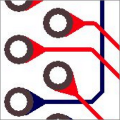
High Speed Signal Routing
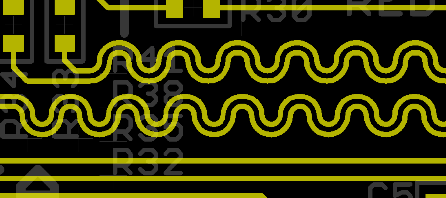
High Speed Routing Design FI
A high-speed signal will take the path of least resistance, therefore 90-degree turns and other connections may cause signal crowding. For RF signals, special attention to layout angles is important. An alternate method to 90-degree angles is to use a rounded trace, or no more than two 45-degree angles to achieve the same intent as a true 90-degree trace turn. For differential pairs, both traces should be kept at the same distance and trace path to maintain impedance. Additionally, stray signal stubs, dangling traces, or ground plane orphans can act as inadvertent antennas which could transmit unwanted signals.
For RF radios and other high-speed systems, signal purity is paramount. Signal loss can happen for several reasons such as impedance mismatch, poor layout routing practices that use unnecessarily long traces and insertion loss of components. Maximum signal power is often needed for transmission and reception, with consumption of supply power kept to a minimum. Identifying PCB areas where attenuation may be a culprit to signal power loss. Where possible, wider traces can be used for lower impedance trace paths within a PCB. Exotic board materials with a lower permittivity may be needed for best EMC. ‘Tear Drop’ layout techniques are often used at signal terminals or vias for signals that exceed 1GHz. The main benefit is to prevent dampen the abrupt discontinuity from the trace impedance to the via, which may be less controlled than the trace. Check out this article for more specifics on high-speed routing design.
Test Information for EMC
Introduction to EMC Compliance 2
There are several key items that need to be described for the EMC test center to be begin to take measurements. First, the wireless radio module used for the RF transmitter incorporated into the system will need to be declared for the testing. This will announce the pre-certified module to be used. Second, the transmit frequency range and highest clock rate within the system will need to be declared. Third, a document or datasheet describing the general theory of operation allows the certification reviewer a method to understand the technical function of the product.
A fourth item to identify is to describe a full system power cycle that covers the power-up sequence, any boot sequence, sleep or idle time, functional operation and power-down. If this is performed in a loop, the amount of time that the system spends in each state should be identified and listed. The performance criteria and the method to detect a failure or incorrect operation should be identified. For example, if an incorrect RF signal is received, a failure LED may blink or an error message may be sent to a screen. Lastly, any non-standard power requirements or RF product emission limits need to be highlighted. This will allow you to work with the EMC test reviewer to identify possible solutions to address any non-compliance performance.
The Testing Center
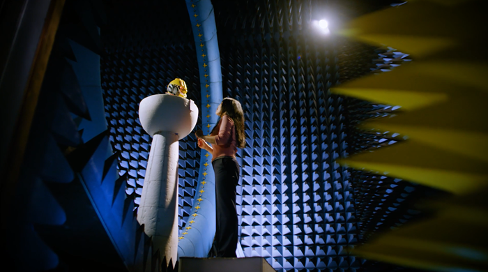
WRC OTA Chamber
An EMC test center will first determine whether your system is intended to transmit or receive RF signals or not. It is also imperative to know the intended frequency spectrum since other ISM bands also exist beside 2.4Ghz. For other licensed spectrum applications such as cellular phones, the frequency spectrum will be purchased and known. The system will be required to operate in all primary modes such as functional, idle, sleep and in a powered down mode.
While operating, a large antenna will scan to identify the transmitted signals from your system and display them on a spectrum analyzer. The spectrum analyzer will show the frequency spectrum and power of any signals, intentional or otherwise, from your system. This information will be compared to the maximum allowed power as identified by the governing body. Any excursions beyond this mask will need to be addressed, either through software configuration or perhaps PCB layout updates. Needless to say, first pass success is worth spending extra time with your CM on critical layout concerns during the PCB design stage.
Prior to formal certification, a system can be tested to ensure compliance in advance. However, test centers use large, expense anechoic RF chambers for EMC testing. Most engineering design centers do not have one of these large anechoic chambers in the back corner of the lab. Therefore, depending upon the size of the system, a smaller RF shielded metal box can be used as a substitute. Cabling and power can be brought into the box through small holes that are blocked with copper inserts. This will, in effect, provide the same shielding as a full anechoic chamber. Whether a large external antenna is needed, or a small PCB chip antenna, the layout and RF routing are key in order to maximize success and pass EMC standards.
EMI & EMC Compliance Conclusions
FCC and CE compliance may seem to just hinder your products development cycle but it is an important process to insure preexisting devices will function correctly with your device in proximity to each other. With the RF spectrum noise floor rising it is important to further test your device to make sure outside interference does not cause your customers problems. Otherwise, your latest IoT gadget may stop working when your customer microwaves dinner.
For engineers looking for EMC testing and support I highly recommend the Wireless Research Center (WRC). The WRC is a testing facility and research hub that offers both engineering and business services to support the commercialization of wireless products from initial concept through high-volume production.
Related Topics
PCB Antenna Design: A Step-by-Step Guide
Step-by-step guide to the PCB antenna design process, providing practical tips to help you successfully integrate the antenna into your wireless product.
Improve Your Next PCB Prototype: Better Debugging, Testing, and Reliability
Enhance PCB prototypes with debugging, testing, and reliability features. Get design tips like test points, power management, and signal integrity testing
Top 10 Electronics Podcasts You Should Listen To
This curated list of top electronics podcasts is tailored for those trying to keep up with the rapidly evolving tech world.
About MacroFab
MacroFab offers comprehensive manufacturing solutions, from your smallest prototyping orders to your largest production needs. Our factory network locations are strategically located across North America, ensuring that we have the flexibility to provide capacity when and where you need it most.
Experience the future of EMS manufacturing with our state-of-the-art technology platform and cutting-edge digital supply chain solutions. At MacroFab, we ensure that your electronics are produced faster, more efficiently, and with fewer logistic problems than ever before.
Take advantage of AI-enabled sourcing opportunities and employ expert teams who are connected through a user-friendly technology platform. Discover how streamlined electronics manufacturing can benefit your business by contacting us today.