It is essential to ensure that the silkscreen is visually accurate when viewing both sides of the PCBA, not just from the top.
PCBA development projects undergo several iterations of review and updating. Changes create revisions that have to be checked recursively to make sure they’re in line with the original design. To stay within Design for Manufacturing (DFM) requirements, final adjustments and cleanup must be done when preparing the design for manufacturing.
Work with your CM partner to plan out a DFM plan before the project is finished. Use your partner’s Design Rule Check (DRC). which will act as a moderator for your PCB design software to constantly check your design for issues as you lay it out. Before sending your final design files to the CM for PCB manufacturing, check out these useful tips and final steps.
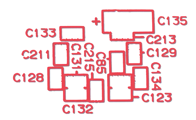
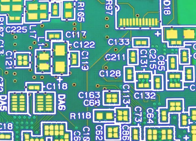
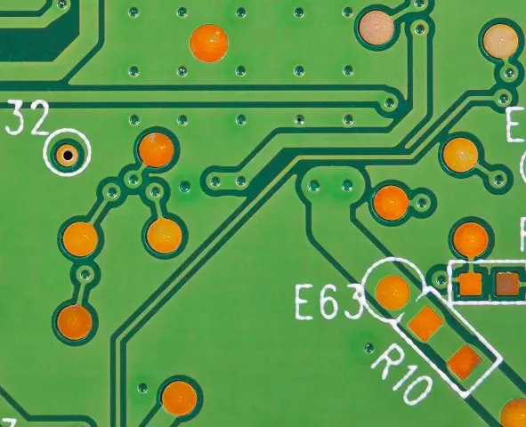
Check Top and Bottom Silkscreens
Automated visual inspections and component designations on printed circuit board assemblies (PCBAs) are often indicated using silkscreens on both the top and bottom sides. During the final design check, it is important to verify that the silkscreen alignment and numbering of passive and active components are correct.
Complex designs may involve mirroring on one side, which can make the silkscreen less useful due to the backward mirroring. Therefore, it is essential to ensure that the silkscreen is visually accurate when viewing both sides of the PCBA, not just from the top.
To avoid overlapping designators, it may be necessary to move silkscreen elements to eliminate this issue. Additionally, ensure that silkscreen elements do not cover solder pads or holes. Adding legend markings, such as company logos and part numbers, can help with product identification.
During the design process, it is also important to consider the location of component outlines, as the silkscreen should be positioned outside of component boundaries to avoid overlap with the component body outlines.
Adjust Routing and Vias
Review the output from the automated routing tool, which identifies any errors or warning messages. It’s important to pay attention to the warnings as well because they could potentially indicate a problem with the design. Make any necessary adjustments to the routing to eliminate any warnings that might suggest a weakness in the design.
Check that the vias on the printed circuit board assembly (PCBA) are the correct drill size, pad size, and tolerance for the holes. In some cases, adding a teardrop shape to a trace can help prevent a neck-down issue. If needed, be sure to include this teardrop shape.
Finally, confirm with the CM (contract manufacturer) that the routing output is ready for manufacturing and does not have any remaining issues.
Double-check Tolerances
It is important to ensure that the design of a printed circuit board assembly (PCBA) adheres to certain mechanical tolerances, such as line width, etching, spacing, and minimum distance requirements. These should be double-checked with the manufacturer before the design is finalized.
The encroachment on the tolerances could be subtle and may get missed until later in the project during characterization or prototyping, precisely when there is no time built into the schedule to correct these issues. Any tolerance update should be identified before sending the design files for initial fabrication.
Configure Your Test Point Requirements
Manufacturing tests are used to check the performance of a Printed Circuit Board Assembly (PCBA) by accessing various points on the board. These points, called test points, need to be carefully planned and included in the design from the start, rather than being added later. It’s best to work with a contract manufacturer (CM) to include test points in the Design for Manufacturability (DFM) plan.
Ideally, every node on the PCBA should have a test point, so that it can be fully tested. A dedicated test point is more reliable and less prone to problems than using a component lead. Test points should be placed throughout the board to allow easy access by the test equipment. A test point can be as simple as a copper pad with a minimum size of 1mm. You can find specific requirements for test points in the DFM plan with your CM.
Perform Mechanical Checks
In the construction industry, a common phrase cited is “Measure twice, cut once”. In the electrical systems industry, the same principle can be applied to the design’s mechanical portion. Mechanical interference points should be vetted for contention based on known mechanical tolerances.
By taking into account the worst-case tolerances for all dimensions, issues can be spotted before the design is complete. Three-dimensional CAD development programs should test for all conditions. The mechanical design and electrical design should always integrate seamlessly.
Visual accuracy is often achieved by using precision alignment reference points known as fiducials. These are often copper circles or specific designs embedded within the PCBA for optical identification. Once the design is complete, the fiducial’s location, the tolerance of its placement, and its coordinates within the design should be verified.
Listen to this classic episode of the Circuit Break Podcast as Parker and Stephen discuss frequency detection and integrated circuit layout with Brian Kaczynski of Second Sound.
Remember all Your Deliverables
Your CM will define the deliverables package needed by the factory to build your system. Your CM partner will need to receive these deliverables from the design team. It is rare that the manufacturer will handle this for you.
Here are some usually required files for PCBA fabrication and assembly:
- Pick-and-place file used in automated assembly
- NC drill files for automated drilling
- Fabrication files
- Testing wire netlist
- Test point report showing test points within the PCBA layout
- Bill of Materials (BOM) with primary and alternate information for each component
- Fabrication and assembly drawings showing how PCBA must be manufactured
- Panel array drawing showing the arrangement of PCBAs within a panel
Working with your CM partner to develop your DFM plan will help you address all your manufacturing concerns throughout the project. Make sure you check all tolerances, test point locations, and mechanical aspects one last time before sending the design to manufacturing. Your CM should inspect the full package of deliverables once it is received. Checklists are a great way to avoid simple mistakes that will slow down your manufacturing process in the long run.
Get your project started today.
Make final checks and edits automatically with the MacroFab technology platform.