Fiducials are Fun!
Fiducials, or fiducial marks (fids for short) are a physical identifier for an imaging system that allows a point of reference. The fid essentially gives the image system a known zero reference point. For PCB assembly, these are generally small marks on the top and bottom layers of copper.
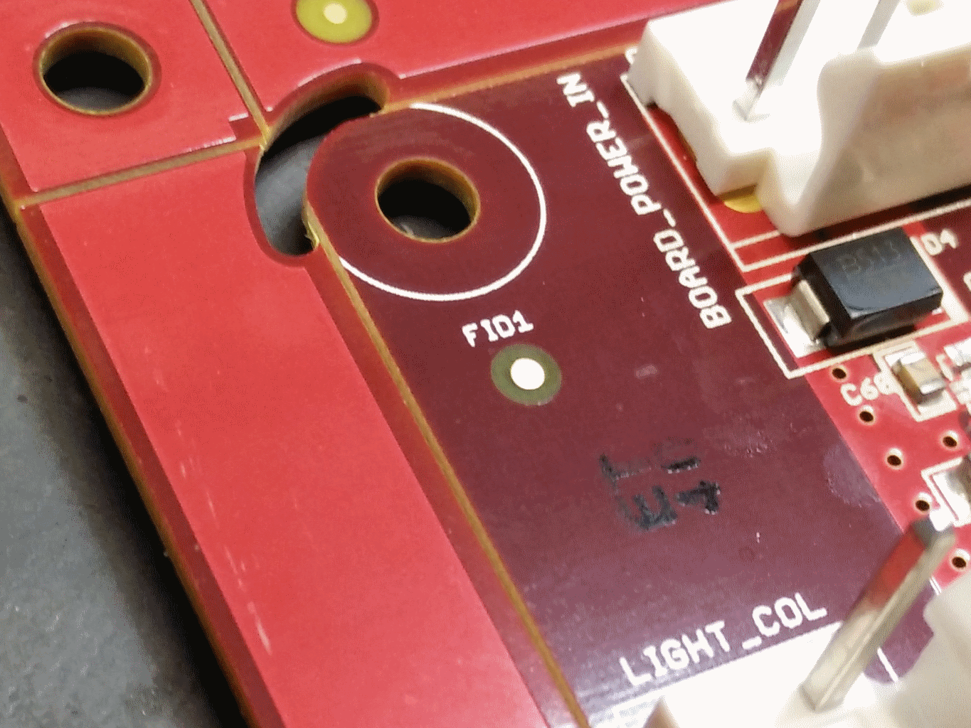
Figure 1: Fiducial as seen by the My200 pick and place.
Explaining Fidicials on a PCB Assembly
Understanding the significance of fiducials in the world of electronics is crucial. They serve as navigational aids for automated assembly equipment, particularly during the pick and place process. The accuracy with which components are placed on a PCB (Printed Circuit Board) depends heavily upon the accuracy with which the machine recognizes the fiducials. By utilizing these marks, the possibility of errors in assembly diminishes, ensuring a smoother manufacturing process.
The pick and place locates the fids and generates an offset from the machine zero to the PCBs fids. Without the fids, the pick and place will not accurately place parts on the board as the board will only be centered by the mechanical stops on the conveyor. Figure 1 shows a 50 mil fid being located by the My200 pick and place.
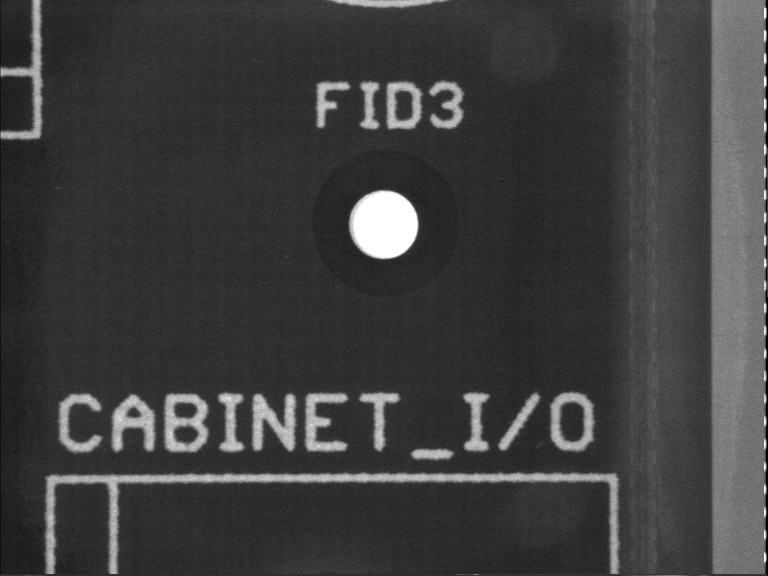
Figure 2: Fiducial mark example on PinHeck PCB.
IMG 20160208 114117 1454953544580
The Importance of PCB Fiducials for Precise Component Placement
The precise nature of fiducials ensures that even if the PCB shifts slightly on the conveyor, the pick-and-place machine can still adjust its operations based on the position of the fids. As a result, they are essential for fine-tuning component placement.
Fiducials are generally 1-2mm or ~50-100 mil in diameter on the copper layer. The copper layer is used instead of the silkscreen because sometimes the silkscreen will be offset from the copper layer. Using the silkscreen as a fid can result in the parts being placed offset from their centers. A pull back of the solder mask is recommended by 2-3mm or ~100-150mil. Most solder mask finishes are glossy which might obscure the boundary between the fid and the solder mask. Pulling back the solder mask increases the contrast of the copper to the surrounding area which increases the level of confidence the machine has in finding the fids.
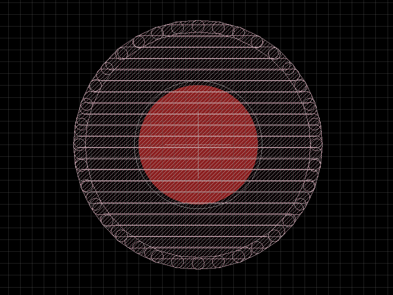
Figure 3: 50 mil Fiducial mark in Eagle.
Fiducial Design for PCB Assemblies: A Beginner's Tutorial
For those just stepping into PCB design or production, it's important to remember that choosing the correct fiducial size and positioning can make a significant difference. Their visibility and contrast enable the machine to detect them with ease, ensuring the correct orientation and positioning of components. Also, different machines and equipment may have different recommendations and requirements for fiducial marks. Check with your CM if you have questions.
Figure 3 shows a 50 mil diameter fid with a 100 mil diameter pull back on the solder mask. This is the same fid as shown in Figure 2. In most EDA tools you can make a fid by placing a round SMD pad. Be sure to remove the paste layer (cream in Eagle) and increase the solder mask resist (stop in Eagle).
Figure 4: Pinheck PCB with 3 board fids and 2 local fids.
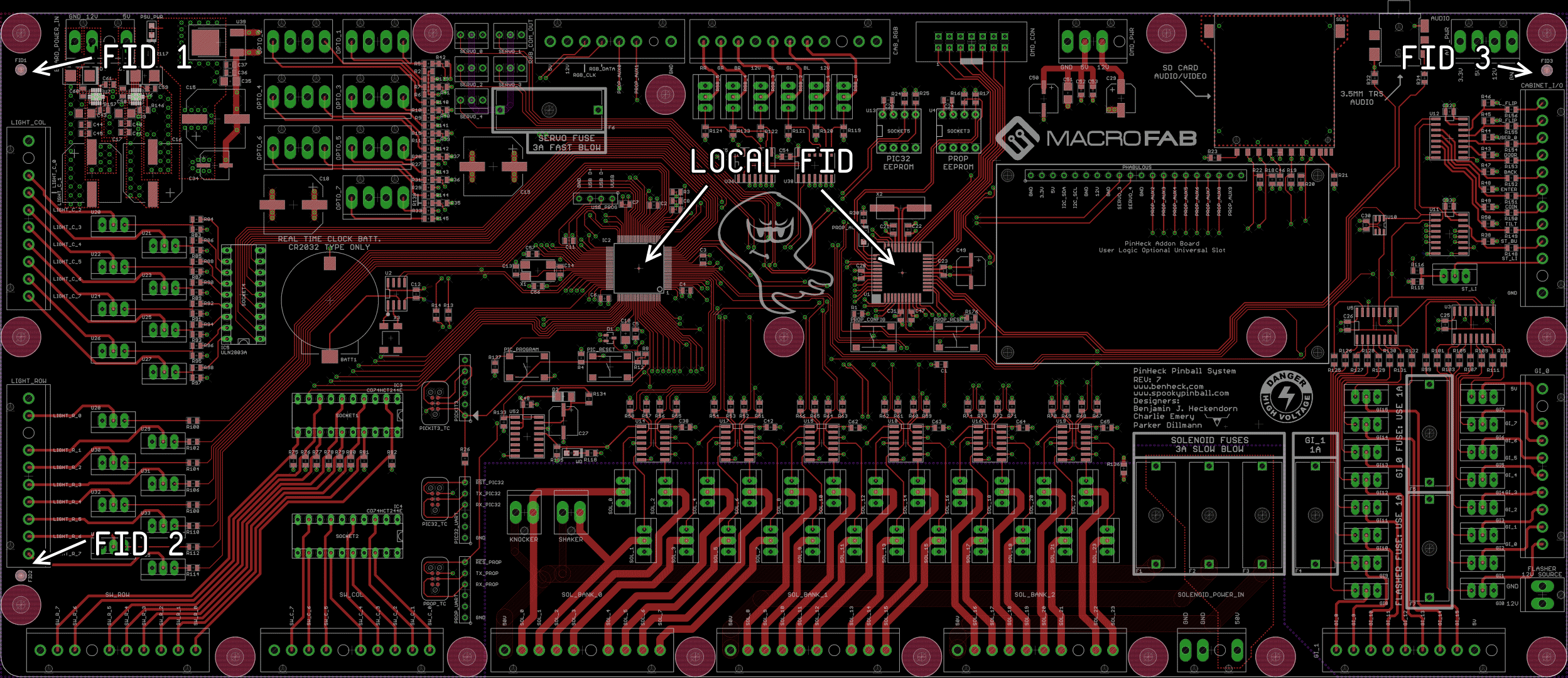
The minimal number of fids per PCB is two but three is preferred. One fid corrects the X-Y location of the board. Two fids corrects any skew of the board in the conveyor. Three fids corrects any shrinking or stretching over the entire PCB. The third fid is generally not important for smaller boards. For larger boards or boards with small parts and features it is highly recommended to keep placement errors low across the entire board.
Figure 5: Center 50 mil fiducial mark on a 0.4mm TQFP-100 PIC32
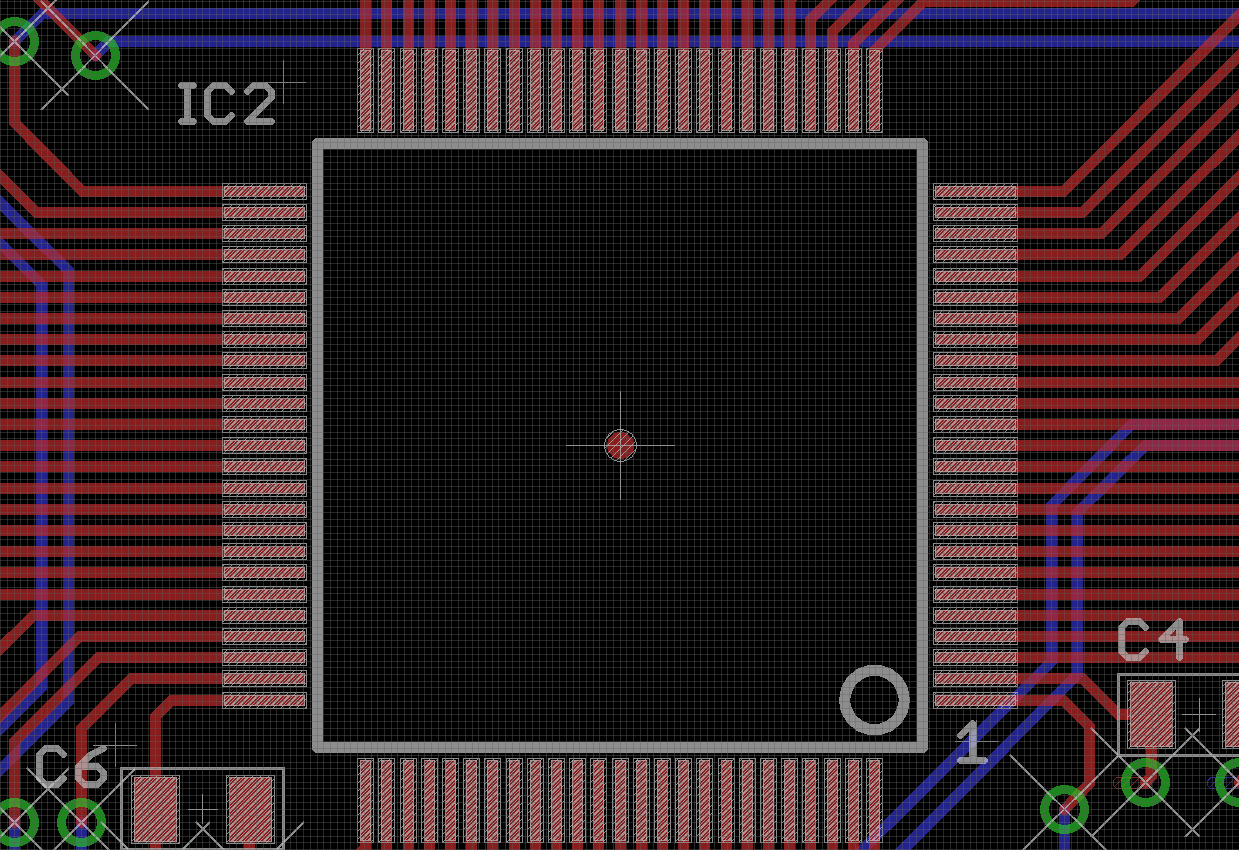
Center Fid Eagle 1454954708121
Maximize PCB Assembly Efficiency with Strategic Fiducial Placement
Given the increasing complexity and miniaturization of electronics, ensuring perfect alignment becomes even more vital. A local fid, like the one shown in Figure 5, can be pivotal in ensuring that larger components are accurately placed. These local fids act as a secondary checkpoint, providing a more localized reference for the placement machines.
Sometimes it's useful to place a local fid in the center of a large IC, as shown in Figure 5. This increases the accuracy of the placement of the part and makes it easy to check if the parts X-Y location data is correct.
A helpful tip is to make the fids a part in your EDA tool, so when you export your XYRS placement data the fids are included. In the value field for the fid you should include the diameter of the fid. In our MF_Aesthetics Eagle Library there are some examples of fids we have used.
In conclusion, fiducials play a pivotal role in modern PCB assembly, ensuring high precision and accuracy. They act as a guide, ensuring every component finds its perfect spot on the board. When designing or working with PCBs, always consider the optimal size, position, and number of fiducials for the best results.
Related Topics
Schematics to Reality: Innovate with Custom PCBs at MacroFab
A glance at how MacroFab's platform can turn concepts into a real functional product. This can be done with the many services that MacroFab offers.
Chinese Tariffs Impact Update: May 13th, 2019
Today, May 10th, 2019, the United States Trade Representative has increased the import duties on Section 301 Tariff: List 3, covering Chinese Tariffs.
Smaller Prototypes Possible with New Standard DRC Specs
Here at MacroFab, we are always striving to improve our service and capabilities we offer. Today we announce smaller Standard DRC Specifications!
About MacroFab
MacroFab offers comprehensive manufacturing solutions, from your smallest prototyping orders to your largest production needs. Our factory network locations are strategically located across North America, ensuring that we have the flexibility to provide capacity when and where you need it most.
Experience the future of EMS manufacturing with our state-of-the-art technology platform and cutting-edge digital supply chain solutions. At MacroFab, we ensure that your electronics are produced faster, more efficiently, and with fewer logistic problems than ever before.
Take advantage of AI-enabled sourcing opportunities and employ expert teams who are connected through a user-friendly technology platform. Discover how streamlined electronics manufacturing can benefit your business by contacting us today.