In modern electronics, it is rare to encounter electronics with few active components. Increasing IC counts in circuits introduces interesting design challenges. In this post, we will discuss bypass capacitors and their role in preventing noise and voltage glitches on power supply rails.
All ICs need power which for most applications is supplied from a single voltage regulator. Powering multiple chips from a single regulator is not as simple as dropping your chips on a PCB and connecting them to the power supply. ICs do not present a constant load on the power supply, instead they have varying loads depending on their function. Since the voltage regulator’s job is to keep its output voltage constant, variations in the load will represent themselves as changing current.
Let’s take a look at some hypothetical (and highly exaggerated) examples of different chips and the current waveforms they demand from the power supply.
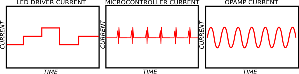
LED Driver: Differing current levels when IC Turns on LEDs
Microcontroller: Current spikes corresponding to the clock frequency
Opamp: Current is proportional to the load it drives
It is not uncommon for a circuit to have a single voltage regulator supplying the example chips above and more. As the complexity of a circuit increases, so does the complexity of the load presented on the power supply.
The Problem:
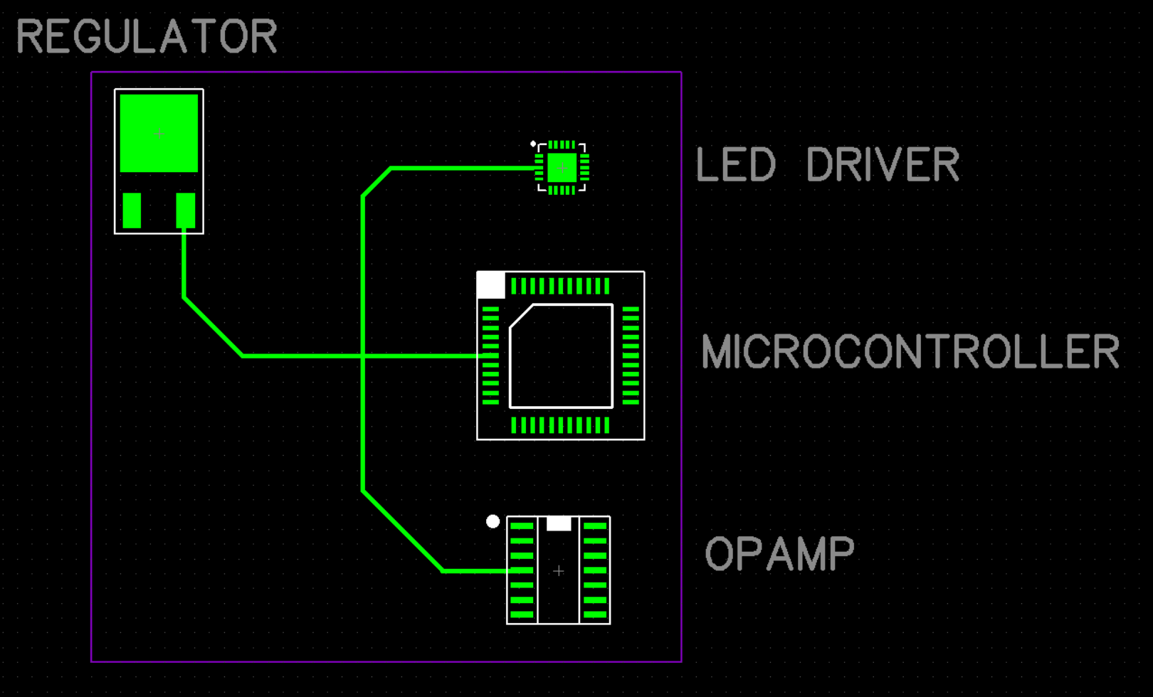
So what happens when we connect all of these chips to the same power supply? Let’s take a look at a theoretical PCB to find out.
This example PCB shows a voltage regulator that supplies power to the three chips mentioned above. Power traces are shown in green stemming from the voltage regulator. (All other traces are not shown for clarity).
In any circuit there will inevitably be some distance between the voltage regulator and the chips that it provides power to. In an ideal world, the copper traces that span the distance between the regulator and ICs would have no impedance and act as a short circuit. In reality, all traces will exhibit some non-zero impedance and will have an impact on the trace voltage when current flows through them.
Considering the current waveforms presented above, as they pass through the impedance of the traces they induce voltage spikes or noise (remember ohm’s law?). This noise is not due to the voltage regulator or the traces picking up stray electromagnetic waves in the environment, but simply due to the chips pulling the current they need to operate – something that they are supposed to do!
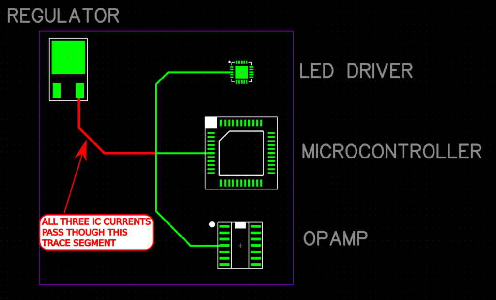
To make matters worse, the way traces are routed on the PCB can compound the issue. On our example PCB, the current that supplies all three ICs is forced to pass through a single trace before splitting into individual traces to the chips. Because the current for all three chips passes through this one segment, the induced noise on this trace is the sum of the induced voltages. The voltage noise that is induced on the trace is then at risk of being coupled into our ICs and potentially anything further down the line.
In this example with only three chips and it is easy to see how this can become an issue. Imagine what would happen if we had more chips pulling more complex current waveforms? It is certainly possible for the induced noise on a power supply line to become large enough to compromise the performance of some if not all of the ICs connected to the supply or the components that are connected themselves to the ICs.
The Solution:
Luckily, the solution to this problem is both cheap and simple. By placing a low impedance path connected to the traces that feed power to the ICs we can create a filter that “bypasses” or “decouples” noise on the supply line. The easiest way to accomplish this is to add a capacitor across the power supply + and – lines. These capacitors are typically called bypass capacitors for reasons that will become clear soon.
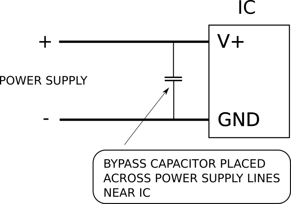
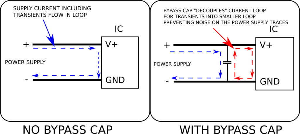
Below is an image of a schematic showing a bypass capacitor connected across the power supply lines near an IC.
Let’s take a look at the effects of a bypass capacitor on the transient current flowing into this IC.
The image on the left shows the flow of current in a circuit that has no bypass cap on the IC. Any transient spikes in current will be subjected to any impedance on the traces and can cause problematic voltage droops or noise.
The image on the right shows the same circuit with a bypass capacitor installed across the power supply lines near the IC. Since the capacitor has the ability to source large currents quickly, the transients can be supplied directly from the capacitor instead of having to be sourced from the power supply. This can be seen with the current loop on the right in red. The addition of this capacitor helps “bypass” the transient current spikes from the voltage regulator and helps keep the voltage on the traces steady by sourcing the quick current transients.
By acting as a local transient current source, the capacitor prevents noise and voltage glitches from being coupled into other ICs that are connected on the power supply traces. Because of this, the capacitors are often called “decoupling capacitors” in addition to the name “bypass capacitor” since they decouple the current demands of one component in the circuit from the rest of the circuit.
It is important to note that the names “decoupling capacitor” and “bypass capacitor” were given to describe the function of the capacitors in the circuit and not a specific part. There are no capacitors that are specifically called decoupling caps or bypass caps as any cap can perform the function although some caps are more suited to the job than others as we will explore later.
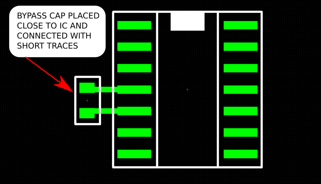
Layout Considerations
Bypass caps should always be placed as close to the power pins as possible. Since the intent of the cap is to provide as low of an impedance path as possible and to decouple the current path for transients, keeping the traces from the cap to the IC short is very important. Every power pin on an IC should be bypassed with its own unique cap.
Bypass Cap Value & Size:
Considering the impedance of the traces on the PCB, the input impedance of the IC, and the operating frequency of the IC, an optimal value of bypass capacitor does exist but going through the rigors of calculating the value is rarely useful or necessary. In many cases the datasheet for an IC will give a recommended value for the capacitor. If no value is suggested, 0.1uF (100nF) is widely accepted as a standard go-to value. For most designs, a standard ceramic 0402, 0603, or 0805 package size will typically work well as a bypass cap.
Recap
Bypass capacitors are an absolute must to avoid issues with noise on power supply traces and cross talk between devices on a PCB. Every IC in your designs should have bypass caps placed close to their power pins to provide low impedance paths for reducing the impact of current transients. Whenever available, it is best to use the manufacturer’s recommended value for the bypass cap’s value.