Microcells and Distributed Antenna Systems (DAS) are critical components of modern wireless networks, addressing coverage and capacity challenges in dense urban, indoor, and complex environments. Traditionally reliant on macrocell infrastructure, wireless service providers have increasingly turned to these technologies to meet surging user demands. The proliferation of smartphones, IoT devices, and data-intensive applications, coupled with the advent of 5G, is driving substantial investment in DAS equipment, anticipated to reach $16 billion by 2027.
End-users demand ubiquitous, high-quality wireless connectivity, unhindered by environmental factors such as building structures or adverse weather conditions. The increasing prevalence of data-intensive applications, including 4K/8K streaming, heightens the need for robust network capacity. To address these challenges, wireless service providers are adopting a complementary approach, integrating microcells and DAS with traditional macrocell infrastructure.
However, DAS applications, like all RF systems, depend on accurate signal propagation. Good signal integrity mostly relies on using meticulously designed high-frequency printed circuit board assemblies (HF PCBAs) within the DAS system’s RF circuitry. This article explains how to design scalable HF PCBAs for various DAS applications, paving the way from traditional macrocells to the microcell-driven future of 5G technology.
The Macrocell Era: A Broad Brush Approach
Mobile communication underpins contemporary life, facilitating tasks ranging from voice calls to internet browsing. This technology relies on cellular networks, partitioning geographic areas into discrete cells. Each cell is equipped with a base station, or cell tower, managing communication within its designated area. The size of a cell is determined by the maximum distance a tower’s signal can reliably reach a device.
High-Frequency circuits-like those utilized in microcells and DAS-are more sensitive to PCB material selection, fabrication, and assembly.
Traditionally, wireless service providers have employed macrocells to provide broad coverage. Macrocells consist of base stations with high-gain antennas mounted on elevated structures, such as towers or tall buildings. This configuration maximizes signal propagation.
Despite their benefits, macrocells have several drawbacks. These are some of the key challenges they present:
-
Growing Need for Bandwidth: As of 2024, 99 percent of U.S. households subscribe to at least one streaming service. Meanwhile, video conferencing has become ubiquitous across a significant portion of the market. The global gaming community, numbering over a billion users, further amplified demand. These figures show a big rise in the need for more bandwidth. Yet, macrocells struggle with spectrum reuse and therefore cannot handle this growing need. Consequently, network congestion in densely populated areas has resulted in diminished speeds and service reliability.
-
Weak Coverage for Some Users: Macrocells are designed for broad geographic coverage, typically employing a single base station tower. While this approach is effective for expansive areas, users situated at the periphery of a cell may experience degraded service quality. Increased signal propagation distances and the presence of obstacles can lead to diminished signal strength, echo, and reduced data rates.
-
Capacity overload in hot spots: In areas with high user density, such as urban centers or event venues, macrocells often struggle to handle the heavy demand for mobile services. These ‘hot spots’ can have too many devices trying to connect to the same cell tower simultaneously, leading to network congestion.
-
Poor indoor coverage: Despite more than half of mobile usage occurring indoors, macrocell systems often exhibit suboptimal performance in indoor environments. Building materials commonly employed in construction, such as concrete and steel, significantly attenuate cellular signals. Furthermore, the attenuation is intensified by the increased distance between the building and the macrocell tower. Consequently, indoor coverage and capacity are severely limited, resulting in unreliable mobile communication within most buildings.
-
5G Limitations: 5G technology uses high-frequency band signals, specifically millimeter waves (mmWaves), which make it possible to send large amounts of data quickly. However, these signals don’t travel very far. They also get easily blocked by buildings, trees, and rain. This makes it hard for 5G signals to be sent and received using macrocells, where cell towers are designed to cover large areas and are often far away from users.
The Rise of Microcells and DAS
Microcells and Distributed Antenna Systems (DAS) represent specialized wireless network solutions designed to augment traditional macrocell infrastructure. These technologies offer a targeted and economically viable approach to enhancing coverage and capacity in both outdoor and indoor settings.
A microcell constitutes a type of small cell network characterized by the deployment of mini-base stations, or nodes. These low-power antennas deliver a capacity comparable to macrocell base stations while serving a significantly smaller geographic area. In urban environments, microcell nodes are often discreetly integrated into existing infrastructure, such as streetlights and utility poles. This aesthetic integration distinguishes microcells from their larger, more conspicuous macrocell counterparts. The advantages of microcells include:
-
Better Coverage: Carriers use microcells to improve coverage in hard-to-reach places, like behind buildings or at the edges of macrocells, where signals often weaken or drop.
-
Capacity Offload: Microcells help to reduce the load on macrocell towers by handling part of the data traffic. This redistribution of traffic significantly increases total network capacity. Also, these nodes are connected via optical fibers, enabling them to manage large volumes of data at high speeds.
-
Enhanced User Experience: Users may be far from macrocells, which have one signal source. Microcell nodes, on the other hand, are strategically placed closer to users across multiple locations. This proximity makes the coverage more stable. Also, in densely populated urban areas, the microcell network densification improves signal quality and capacity, giving users better service.
-
Supports 5G: Microcell antennas use mid-band and high-band frequency signals (millimeter waves) and are positioned nearer to users, making them more suitable for 5G networks compared to macrocells. For example, in 2020, Verizon deployed many microcell nodes to support what it calls its “5G Ultra Wideband” service.
-
Blends Better with City Infrastructure: Microcell nodes are less noticeable than macrocell towers and can be easily added to cities. This makes them very useful in places with strict zoning rules. Or, in densely populated cities like New York, where installing a large macrocell tower might be impractical due to space limitations. Microcells are a discreet and efficient way to increase network capacity and coverage.


DAS, on the other hand, is primarily used to provide reliable indoor wireless service in venues where signals from external cell towers cannot penetrate effectively.
Carriers deploy DAS in high-capacity venues such as stadiums and airports. They also use it to improve coverage in places that are hard to reach, like subways and tunnels. Different types of DAS are tailored for specific settings, from homes and small offices to large public spaces and major airports.
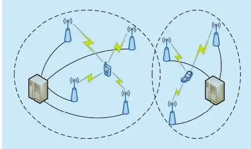
The DAS starts with a signal source, which can be cellular signals from an outdoor antenna that picks up signals from nearby cell towers or direct feeds from a microcell base station. This primary signal, known as the donor signal, is then distributed throughout localized areas via antenna nodes.
These nodes are strategically placed throughout the area to provide even coverage. This could include places like individual floors of a building, specific rooms, or outdoor spaces within a complex.
One of the primary benefits of DAS is that the antenna nodes are placed close to users. This shorter transmission distance helps reduce signal attenuation. The antenna nodes are also simple, inexpensive, and power-efficient.
Another significant advantage of DAS is its ability to provide high spatial diversity gain. The system can send and receive signals over multiple paths. This improves the reliability and quality of communication. It also supports flexible and efficient resource management, adapting to different user demands and conditions for optimal performance.
Compare and Contrast: DAS vs. Microcells
While both DAS and microcells are designed to improve cellular coverage in specific areas, they have distinct characteristics and applications. DAS, characterized by a centralized architecture, is optimized for expansive coverage areas and high user capacities, making it suitable for large venues. Conversely, microcells employ a standalone approach, offering more localized coverage and are typically deployed in smaller spaces. Regarding flexibility, DAS supports multiple carriers while microcells tend to be carrier-specific. Though distinct, these technologies can be complementary, providing comprehensive wireless coverage in complex environments. Here’s a breakdown of key differences:
Distributed Antenna System (DAS) |
Microcells |
|
|---|---|---|
| Network architecture | Point-to-multipoint. | Point-to-point. |
| Coverage area | Larger, often encompassing entire buildings or outdoor venues. | Smaller, typically covering a single floor or a small outdoor area. |
| Antennas | Multiple antennas connected to a central headend. | Single or multiple antennas, but with a simpler setup than DAS. |
| Capacity | Higher capacity, capable of handling large numbers of users simultaneously. | Lower capacity compared to DAS, but still sufficient for most indoor environments. |
| Flexibility | Can be shared by multiple carriers, offering neutral host opportunities. | Often carrier-specific, but some models support multiple carriers. |
| Complexity | Generally more complex to install and manage due to the distributed nature. | Simpler to install and manage compared to DAS. |
The Challenge of High-Frequency PCBAs in MicroCells and DAS
Microcells and DAS systems benefit from using mid-band and high-band frequencies (mmWaves) to deliver fast data speeds and increased capacity. However, high-frequency circuits–like those utilized in microcells and DAS–are more sensitive to PCB material selection, fabrication, and assembly. Thus, developing HF PCB assemblies for microcells and DAS systems will likely present the following issues:
-
Impedance mismatch sensitivity: At high frequencies, the PCB trace must be treated as a transmission line due to dominant AC characteristics like impedance, inductance, and capacitance. Impedance mismatches among the transmission line, source, and receiver can cause signal errors. These include signal overshoot, undershoot, and ringing.
-
Transmission loss due to dielectric absorption: High-frequency signals excite polarized molecules in the substrate, causing the substrate to absorb and convert some of the signal energy to heat. This absorption decreases signal strength.
-
Signal attenuation due to skin effect: At high frequencies, the current flows mainly through a thin layer on the surface of the conductor. This is called the ‘skin’ of the conductor. Because the current is limited to this outer layer, the resistance of the PCB trace increases. This higher resistance leads to more signal attenuation.
-
Crosstalk: Crosstalk refers to the unwanted coupling of signals between neighboring traces on a PCB assembly. This issue is particularly common in complex circuits, such as those found in microcells and DAS, which often require densely packed, multilayer PCBs.
-
Highly sensitive to conductor roughness: The surfaces of conductors on PCB assemblies are not perfectly smooth. This roughness increases the conductor’s resistance, slowing the signal velocity and altering the signal’s phase angle response. These effects are more noticeable at higher operating frequencies.
-
Thermal Issues: As frequency increases, more heat is generated due to more skin effect. Heat also comes from core losses in inductors and transformers and from switching losses in high-speed transistors. If this heat buildup is not regulated, it will lower the dielectric constant of the PCB’s dielectric layer. This decrease changes the PCB’s impedance and affects signal integrity

Designing Scalable HF PCBAs for Diverse DAS Applications
Here are some important considerations to keep in mind when designing PCB assemblies for microcells and DAS to handle high-frequency signals.
Design Factor |
Design Tips |
|---|---|
| Material Selection | Choose a dielectric with a low-loss tangent to minimize signal loss and maximize power delivery.
Choose a dielectric with a low dielectric constant for fast signal propagation. Choose a dielectric that maintains consistent loss tangent and dielectric constant across temperature variations and the application’s bandwidth. Use smooth, low-profile copper to decrease conductor loss, maintain faster signal velocity, and reduce phase angle response changes. To avoid unwanted resonances, keep dielectric thickness and conductor width below one-tenth of the wavelength at the frequency of interest. |
| Fabrication & Assembly Process | Enig finishes can be used in some DAS applications, but other options may provide better performance. Avoid ENIG finishes if variations in Ni-plated thickness alter phase angle response too much. Use smoother plating alternatives like immersion tin (ImSn) or immersion silver (ImAg) instead.
Ensure the fabrication process is well-controlled. Variations in conductor geometry, dielectric thickness, and dielectric properties during mass production can cause impedance mismatches in the PCB and alter the phase angle response. Reduce crosstalk by routing all traces perpendicular to each other, increasing the distance between layers, minimizing the gap between the signal and reference layers, and using differential routing techniques where possible. To reduce impedance mismatches, understand and appropriately apply termination schemes. |
| Thermal Management | Incorporate heat sinks, heat pipes, copper coins or inlays, and thermal vias to efficiently dissipate heat.
Consider using thermally conductive materials for the PCB substrate to enhance heat management. |
| Testing and Validation | Before fabricating your PCB boards, use signal integrity (SI) tools with strong capabilities to simulate and predict how impedance mismatches, crosstalk, inductance, propagation delays, and other factors will affect signal performance.
|

Conclusion
As the demand for high-speed data continues to escalate, 5G has emerged as the vanguard of wireless communication technology. Characterized by its promise of enhanced data rates (up to 20 Gbps), increased capacity, reduced latency, improved reliability, flexibility, and advanced device-to-device communication, 5G systems are driving the evolution of wireless networks. To maintain a competitive edge, carriers are increasingly integrating microcells and DAS into their infrastructure to support 5G deployment.
The realization of high-capacity, low-latency, and flexible 5G systems necessitates meticulous HF PCBA design within microcell and DAS components. This article has explored the critical design considerations and challenges associated with HF PCB assemblies in these applications.
To successfully navigate the complexities of HF PCBA manufacturing, establishing a partnership with a skilled and experienced manufacturing partner is essential. A qualified manufacturer can provide the necessary expertise, resources, and capacity to produce high-quality HF PCBAs that meet stringent performance requirements and adhere to tight production timelines.
Stop chasing updates, and start making progress.